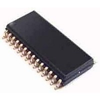
NCV7608DWR2G ON Semiconductor, NCV7608DWR2G Datasheet

NCV7608DWR2G
Specifications of NCV7608DWR2G
Available stocks
Related parts for NCV7608DWR2G
NCV7608DWR2G Summary of contents
Page 1
NCV7608 Octal Configurable Low/High Side Driver The NCV7608 integrates 8 output drivers configurable in any combination of high−side, low−side, or H−Bridge configurations. The integrated standard Serial Peripheral Interface (SPI) allows digital control of all output stages and provides diagnostic fault ...
Page 2
VCC VS Bias + EN Supply monitoring IN5 IN6 IN7 IN8 CSB SCLK SPI SI SO GND Figure 1. Block Diagram (See Figure 2 for detailed diagram) http://onsemi.com ...
Page 3
VCC Core Functions + EN Supply Monitoring IN5 IN6 IN7 IN8 CSB SCLK SI SO GND Overtemp Channels 1&2 Figure 2. Detailed Block Diagram VS Charge Pump Gate Drive Control Slew Rate Control Channels 5-8 VS Charge Pump Gate Drive ...
Page 4
PACKAGE PIN DESCRIPTION Pin # Symbol 1 D2 Drain of configurable driver # Source of configurable driver # Source of configurable driver # Drain of configurable driver #1 5 CSB SPI Chip Select “Bar” ...
Page 5
MAXIMUM RATINGS (Voltages are with respect to device substrate) Rating Digital supply input voltage ( Battery supply input voltage (VS) DC input supply voltage Transient input supply voltage Digital I/O pin voltage (IN5, IN6, IN7, IN8, SI, SO, ...
Page 6
ELECTRICAL CHARACTERISTICS (−40°C < T specified) Characteristic Symbol GENERAL PARAMETERS VS Supply Current Standby (Note 5) IQVS85 Run (Note 6) IVSop VCC Supply Current Standby (Note 7) IQVCC Run IVCCop VCC Power−on reset Threshold VCCPOR VCC Power−on reset Hysteresis VCChys ...
Page 7
ELECTRICAL CHARACTERISTICS (−40°C < T specified) Characteristic Symbol OUTPUT CLAMPS Output clamp Voltage VOCLS Drain with respect to Source Output clamp Voltage VOCHS Source with respect to GND POWER OUTPUTS, AC CHARACTERISTICS Low Side Rise Time T_LSr Low Side Fall ...
Page 8
CSB High−Side Low−Side TDON S Serial Turn On Figure 3. INx High−Side Low−Side TDON P Figure 5. Parallel Turn On INx EN END HS LS Figure 7. EN Delay Time CSB T_HSv High−Side Low−Side T_LSf Figure 4. Serial Turn Off ...
Page 9
Table 1. DIGITAL INTERFACE CHARACTERISTICS Characteristic Digital Input High Threshold Digital Input Low Threshold Input Pulldown Resistance (EN, SI, SCLK, IN5, IN6, IN7, IN8) Input Pullup Resistance (CSB) CSB Leakage Input Capacitance (Note 12) SO – Output ...
Page 10
CSB CSS UP SCLK CLK H CLK SUP CSB SO CStSOf SI SIH SCLK SISUP SOV SO Figure 9. Detailed SPI Timing CLK L http://onsemi.com 10 CLK SUP CS H CSS UP CStSOv ...
Page 11
TYPICAL PERFORMANCE CHARACTERISTICS 1 ...
Page 12
TYPICAL PERFORMANCE CHARACTERISTICS 5.0 4.5 4 3. 5. 1.5 1.0 VS ...
Page 13
Normal Operation Power Outputs The NCV7608 provides eight independent power transistors with pins D1−D8, and S1−S8 as drain and source outputs respectively. For High−side Drive configurations (sourcing), the drain pins are connected to the battery supply. In Low−Side configurations (sinking), ...
Page 14
Table 2. SPI INPUT / OUTPUT Input Data Bit Number Bit Description 15 Driver 8 Open Diagnostic Enable 14 Driver 7 Open Diagnostic Enable 13 Driver 6 Open Diagnostic Enable Driver 6 Open Diagnostic Enable 12 Driver 5 Open Diagnostic ...
Page 15
SPI Input Driver Enable (bits 0−7) A zero turns the driver off. A one turns the driver on. Open Load Diagnostic (bits 8−15) A zero programming bit disables the detection of an open load condition. A one programming bit enables ...
Page 16
INx = 0 deactivates the output stage. Special attention should be paid to detection of over current and open load conditions when operated in a pwm mode. These faults are detected in a 100 ms (typ) time Handling of Fault ...
Page 17
Start No Current Driver ON Yes Limit No No Open Load No Thermal Warning Yes TFOL No Thermal Shutdown CSB Yes No Report VS Power Fault Supply Fail Fault Reported on SO Fault Filters The NCV7608 detects ...
Page 18
Overtemperature shutdown is a latched event. Since thermal warning precedes an overtemperature shutdown, software polling of this bit will allow for load control and possible prevention of overtemperature shutdown conditions. Thermal Warning ...
Page 19
Figure 28. Open Load Circuitry as Low Side Driver Open Load Diagnostic Performance System design sometimes requires open load diagnostics to be turned off to prevent unintended operation. Input Bits 8−15 control this function. One application example would be driving ...
Page 20
Equal diagnostic currents would result in unpredictable results due to process variation. Timing Information Open Load Open Load is reported if open load is enabled and an open load fault exists. OL enabled OL enabled CSB Driver Off* ...
Page 21
CSB Driver Fault TW is detected No TW Driver continues to run detected Driver On CSB SO TSD (T > 175°C) Driver Off Figure 33. Thermal Shutdown Timing Diagram Power Supply Fail VS Overvoltage (OV) or undervoltage ...
Page 22
... COPPER HEAT SPREADER AREA (mm Figure 35. q vs. Copper Heat Spreader JA ORDERING INFORMATION Device NCV7608DWR2G †For information on tape and reel specifications, including part orientation and tape sizes, please refer to our Tape and Reel Packaging Specifications Brochure, BRD8011/D. Figure 34. Power Supply Fail Timing Diagram 1.80 1.70 1 ...
Page 23
... *For additional information on our Pb−Free strategy and soldering details, please download the ON Semiconductor Soldering and Mounting Techniques Reference Manual, SOLDERRM/D. ON Semiconductor and are registered trademarks of Semiconductor Components Industries, LLC (SCILLC). SCILLC reserves the right to make changes without further notice to any products herein. SCILLC makes no warranty, representation or guarantee regarding the suitability of its products for any particular purpose, nor does SCILLC assume any liability arising out of the application or use of any product or circuit, and specifically disclaims any and all liability, including without limitation special, consequential or incidental damages. “ ...


