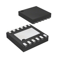
MIC5316-F4CYMT TR Micrel Inc, MIC5316-F4CYMT TR Datasheet - Page 10

MIC5316-F4CYMT TR
Manufacturer Part Number
MIC5316-F4CYMT TR
Description
Low Vin/Vout Dual 300mA LDO With VSC + POR In 2.5mm X 2.5mm TMLFr
Manufacturer
Micrel Inc
Datasheet
1.MIC5316-F5CYMT_TR.pdf
(14 pages)
Specifications of MIC5316-F4CYMT TR
Regulator Topology
Positive Fixed
Voltage - Output
1.5V, 1.2/1V
Voltage - Input
1.7 ~ 5.5 V
Voltage - Dropout (typical)
0.085V @ 300mA
Number Of Regulators
2
Current - Output
300mA
Current - Limit (min)
350mA
Operating Temperature
-40°C ~ 125°C
Mounting Type
Surface Mount
Package / Case
12-TMLF®
Lead Free Status / RoHS Status
Lead free / RoHS Compliant
Other names
576-3145-2
Application Information
The MIC5316 is a high performance, dual low input
voltage,
applications requiring very fast transient response. The
MIC5316 utilizes two input supplies (V
significantly reducing the dropout voltage.
The MIC5316 regulator is fully protected from damage
due to fault conditions, offering linear current limiting and
thermal shutdown.
Bias Supply Voltage
V
the control portion of the MIC5316. Bypassing on the
bias pin is recommended to improve performance of the
regulator during line and load transients. A 1µF ceramic
capacitor from V
reduce the high frequency noise from being injected into
the control circuitry.
Input Supply Voltage
V
independently. The minimum input voltage is 1.7V
allowing conversion from low voltage supplies. The low
input voltage provides high efficiency by reducing the
input to output voltage step which minimizes the
regulator power loss.
Input Capacitor
The MIC5316 is a high-performance, high bandwidth
device. Therefore, it requires a well-bypassed input
supply for optimal performance. A 1µF capacitor is
required from the input-to-ground to provide stability.
Low-ESR
performance at a minimum of space. Additional high-
frequency capacitors, such as small-valued NPO
dielectric-type capacitors, help filter out high-frequency
noise and are good practice in any RF-based circuit.
X5R or X7R dielectrics are recommended for the input
capacitor. Y5V dielectrics lose most of their capacitance
over temperature and are therefore, not recommended.
Output Capacitor
The MIC5316 requires an output capacitor of 1µF or
greater to maintain stability. The design is optimized for
use with low-ESR ceramic chip capacitors. High ESR
capacitors may cause high frequency oscillation. The
output capacitor can be increased, but performance has
been optimized for a 1µF ceramic output capacitor and
does not improve significantly with larger capacitance.
X7R/X5R
recommended
performance. X7R-type capacitors change capacitance
by 15% over their operating temperature range and are
the most stable type of ceramic capacitors. Z5U and
Y5V dielectric capacitors change value by as much as
Micrel, Inc.
July 2008
BIAS
IN1
, requiring relatively light current, provides power to
and V
ultra-low
IN2
dielectric-type
ceramic
, provide the supply to power the LDOs
BIAS
because
-to-ground is recommended to help
dropout
capacitors
ceramic
of
regulator
their
provide
capacitors
IN
designed
temperature
and V
optimal
BIAS
are
for
),
10
50% and 60%, respectively, over their operating
temperature ranges. To use a ceramic chip capacitor
with Y5V dielectric, the value must be much higher than
an X7R ceramic capacitor to ensure the same minimum
capacitance over the equivalent operating temperature
range.
Bypass Capacitor
A capacitor can be placed from the bypass pin-to-ground
to reduce the output voltage noise. The capacitor
bypasses the internal reference. A 0.01µF capacitor is
recommended for applications that require low-noise
outputs. The bypass capacitor can be increased, further
reducing noise and improving PSRR. Turn-on time
increases
capacitance. A unique, quick-start circuit allows the
MIC5316 to drive a large capacitor on the bypass pin
without significantly slowing turn-on time.
No-Load Stability
Unlike many other voltage regulators, the MIC5316 will
remain stable and in regulation with no load. This is
especially
applications.
Enable/Shutdown
The MIC5316 is provided with dual active-high enable
pins
independently. Forcing the enable pin low disables the
regulator and sends it into a “zero” off-mode-current
state. In this state, current consumed by the regulator
goes nearly to zero. Forcing the enable pin high enables
the output voltage. The active-high enable pin uses
CMOS technology and the enable pin cannot be left
floating;
indeterminate state on the output.
Power On Reset
The second regulator (LDO2) provides a Power On
Reset (POR2) status pin.
output. When LDO2 is enabled an active low POR2
indicates an under voltage condition on V
The POR2 status signal can be programmed for a delay
(1sec/µF) by adding a capacitor from the C
ground. Zero delay is added by leaving the C
open circuit.
Voltage Select
The MIC5316 incorporates voltage select technology to
set LDO2’s voltage output to a preset lower level. The
/VSC2 pin is an active low input. A logic high signal sets
V
sets V
OUT2
OUT2
to the full output voltage; while a logic low signal
that
a
to the lower output voltage.
slightly
important
allow
floating
each
with
enable
in
regulator
respect
CMOS
This pin is an open drain
pin
RAM
may
to
to
M9999-070208-A
OUT2
be
the
.
cause
SET2
MIC5316
keep-alive
disabled
SET2
bypass
pin to
pin
an


