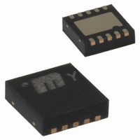
MIC2205-1.85YML TR Micrel Inc, MIC2205-1.85YML TR Datasheet - Page 12

MIC2205-1.85YML TR
Manufacturer Part Number
MIC2205-1.85YML TR
Description
2MHz Synchronous Buck Regulator - Low Q Mode ( )
Manufacturer
Micrel Inc
Type
Step-Down (Buck)r
Datasheet
1.MIC2205YML_TR.pdf
(16 pages)
Specifications of MIC2205-1.85YML TR
Internal Switch(s)
Yes
Synchronous Rectifier
Yes
Number Of Outputs
1
Voltage - Output
1.85V
Current - Output
600mA
Frequency - Switching
2MHz
Voltage - Input
2.7 ~ 5.5 V
Operating Temperature
-40°C ~ 125°C
Mounting Type
Surface Mount
Package / Case
10-MLF®, QFN
Lead Free Status / RoHS Status
Lead free / RoHS Compliant
Power - Output
-
Lead Free Status / RoHS Status
Lead free / RoHS Compliant
Other names
MIC2205-1.85YMLTR
MIC2205-1.85YMLTR
MIC2205-1.85YMLTR
Functional Description
VIN
VIN provides power to the MOSFETs for the switch
mode regulator section, along with the current
limiting sensing. Due to the high switching speeds, a
1µF capacitor is recommended close to VIN and the
power ground (PGND) pin for bypassing. Please
refer to layout recommendations.
AVIN
Analog V
section and the bias through an internal 6 Ohm
resistor. AVIN and VIN must be tied together.
Careful layout should be considered to ensure high
frequency switching noise caused by VIN is reduced
before reaching AVIN.
LDO
The LDO pin is the output of the linear regulator and
should be connected to the output. In LOWQ mode
(LOWQ<1.5V), the LDO provides the output voltage.
In PWM mode (LOWQ>1.5V) the LDO pin is high
impedance.
EN
The enable pin provides a logic level control of the
output. In the off state, supply current of the device
is greatly reduced (typically <1µA). Also, in the off
state, the output drive is placed in a "tri-stated"
condition, where both the high side P-channel
Mosfet and the low-side N-channel are in an “off” or
non-conducting state. Do not drive the enable pin
above the supply voltage.
LOWQ
The LOWQ pin provides a logic level control
between the internal PWM mode and the low noise
linear regulator mode. With LOWQ pulled low
(<0.5V), quiescent current of the device is greatly
reduced by switching to a low noise linear regulator
mode that has a typical I
mode the output can deliver 60mA of current to the
output. By placing LOWQ high (>1.5V), this
transitions the device into a constant frequency
PWM buck regulator mode. This allows the device
the ability to efficiently deliver up to 600mA of output
current at the same output voltage.
BIAS
The BIAS pin supplies the power to the internal
power to the control and reference circuitry. The bias
is powered from AVIN through an internal 6Ω
resistor. A small 0.1µF capacitor is recommended
for bypassing.
March 2005
IN
(AVIN) provides power to the LDO
Q
of 18µA. In linear (LDO)
12
FB
The feedback pin (FB) provides the control path to
control the output. For adjustable versions, a resistor
divider connecting the feedback to the output is used
to adjust the desired output voltage. The output
voltage is calculated as follows:
A feedforward capacitor is recommended for most
designs using the adjustable output voltage option.
To reduce battery current draw, a 100K feedback
resistor is recommended from the output to the FB
pin (R1). Also, a feedforward capacitor should be
connected between the output and feedback (across
R1). The large resistor value and the parasitic
capacitance of the FB pin can cause a high
frequency pole that can reduce the overall system
phase margin. By placing a feedforward capacitor,
these
Feedforward capacitance (C
follows:
For fixed options A feed forward capacitor from the
output to the FB pin is required. Typically a 100pF
small ceramic capacitor is recommended
SW
The switch (SW) pin connects directly to the inductor
and provides the switching current nessasary to
operate in PWM mode. Due to the high speed
switching on this pin, the switch node should be
routed away from sensitive nodes.
PGND
Power ground (PGND) is the ground path for the
high current PWM mode. The current loop for the
power ground should be as small as possible and
separate from the Analog ground (AGND) loop.
Refer to the layout considerations for more details.
SGND
Signal ground (SGND) is the ground path for the
biasing and control circuitry. The current loop for the
signal ground should be separate from the Power
ground
considerations for more details.
where V
V
OUT
C
effects
FF
= V
(PGND)
=
REF
REF
2
π
×
×
is equal to 1.0V.
R1
⎛
⎜
⎝
R2
can
R1
×
1
160kHz
loop.
+ 1
⎞
⎟
⎠
be
Refer
FF
significantly
) can be calculated as
to
www.micrel.com
M9999-031105
the
reduced.
layout


