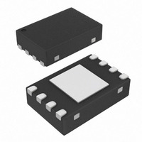
MCP98242T-BE/MNY Microchip Technology, MCP98242T-BE/MNY Datasheet - Page 29

MCP98242T-BE/MNY
Manufacturer Part Number
MCP98242T-BE/MNY
Description
IC,TEMPERATURE SENSOR,LLCC,8PIN,PLASTIC
Manufacturer
Microchip Technology
Datasheets
1.MCP98242T-CEMC.pdf
(56 pages)
2.MCP98242T-CEMC.pdf
(6 pages)
3.MCP98242T-BEMUY.pdf
(48 pages)
Specifications of MCP98242T-BE/MNY
Function
Temp Monitoring System (Sensor)
Topology
ADC (Sigma Delta), Register Bank
Sensor Type
Internal
Sensing Temperature
-40°C ~ 125°C
Output Type
I²C™/SMBus™
Output Alarm
Yes
Output Fan
Yes
Voltage - Supply
3 V ~ 3.6 V
Operating Temperature
-40°C ~ 125°C
Mounting Type
Surface Mount
Package / Case
8-DFN
Full Temp Accuracy
+/- 2 C
Digital Output - Bus Interface
Serial (2-Wire, I2C)
Maximum Operating Temperature
+ 125 C
Minimum Operating Temperature
- 40 C
Lead Free Status / RoHS Status
Lead free / RoHS Compliant
Lead Free Status / RoHS Status
Lead free / RoHS Compliant
Other names
MCP98242T-BE/MNY
MCP98242T-BE/MNYTR
MCP98242T-BE/MNYTR
Available stocks
Company
Part Number
Manufacturer
Quantity
Price
Company:
Part Number:
MCP98242T-BE/MNY
Manufacturer:
MICROCHIP
Quantity:
12 000
5.3.3
The MCP98242 has a Software Write-Protect (SWP)
feature that allows the lower half array (addresses
00h - 7Fh) to be write-protected or permanently write-
protected (PWP). The write protected area can be
cleared by sending Clear Write Protect (CWP)
command. However, once the PWP is executed the
protected memory can not be cleared. The device will
not respond to the CWP command.
TABLE 5-3:
TABLE 5-4:
© 2008 Microchip Technology Inc.
Note:
Note:
Permanently
Protected
Protected
Protected
Status
PWP (Note)
SWP
EEPROM
with
Not
SWP
CWP
WRITE PROTECTION
X is defined as ‘don’t care’.
The Address Pins are ‘X’ or don’t cares. However, the slave address bits need to match the address Pins.
WRITE PROTECT DEVICE ADDRESSING
DEVICE RESPONSE WHEN WRITING DATA OR ACCESSING SWP/CWP/PWP
Page/byte write lower 128 bytes
Page/byte write lower 128 bytes
SWP/CWP/PWP
SWP/CWP/PWP
Page/byte write
Operation
Command
WRITE
WRITE
WRITE
READ
READ
READ
SWP
CWP
PWP
GND GND V
GND V
A2
X
Address Pins
A1
NoACK
NoACK
X
DD
ACK
ACK
ACK
ACK
ACK
ACK
ACK
V
HI_A0
HI_A0
A0
X
To access write protection, the device address code of
the Address Byte is set to ‘0110’ instead of ‘1010’. The
‘1010’ Address code is used to access the memory
area and the ‘0110’ address code is used to access the
write protection. Once the device is write protected it
will not acknowledge certain commands.
shows the corresponding Address Bytes for the write
protect feature.
Address
Address
Address
Address
X
X
X
X
X
Address Code
0110
0110
0110
NoACK
NoACK
ACK
ACK
ACK
ACK
ACK
ACK
ACK
Data Byte
Address Byte
Data
Data
Data
A2
X
X
X
X
X
Slave Address
X
0
0
MCP98242
A1
X
0
1
NoACK
NoACK
NoACK
NoACK
ACK
ACK
ACK
ACK
ACK
DS21996B-page 29
A0
X
1
1
Write Cycle
Table 5-3
Yes
Yes
Yes
Yes
No
No
No
No
R/W
0
1
0
1
0
1


