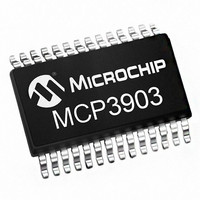
MCP3903-E/SS Microchip Technology, MCP3903-E/SS Datasheet - Page 34

MCP3903-E/SS
Manufacturer Part Number
MCP3903-E/SS
Description
Six Channel Energy Meter Front End, SPI Interface 28 SSOP .209in TUBE
Manufacturer
Microchip Technology
Series
-r
Datasheet
1.MCP3903-ISS.pdf
(54 pages)
Specifications of MCP3903-E/SS
Featured Product
MCP3903 Six Channel ÎΣ A/D Converter
Number Of Bits
24
Number Of Channels
6
Power (watts)
-
Voltage - Supply, Analog
4.5 V ~ 5.5 V
Voltage - Supply, Digital
2.7 V ~ 3.6 V
Package / Case
28-SSOP (0.209", 5.30mm Width)
Lead Free Status / Rohs Status
Lead free / RoHS Compliant
Available stocks
Company
Part Number
Manufacturer
Quantity
Price
Company:
Part Number:
MCP3903-E/SS
Manufacturer:
MICROCHIP
Quantity:
1 200
Company:
Part Number:
MCP3903-E/SS
Manufacturer:
MICROCHIP
Quantity:
12 000
MCP3903
FIGURE 6-7:
6.10
To ensure that all channel ADC data are present at the
same time for SPI read, regardless of phase delay set-
tings for either or both channels, there are two sets of
latches in series with both the data ready and the ‘read
start’ triggers.
The first set of latches holds each output when data is
ready and latches both outputs together when
DRMODE<1:0>=00. When this mode is on, both ADCs
work together and produce one set of available data
after each data ready pulse (that corresponds to the
lagging ADC data ready). The second set of latches
ensures that when reading starts on an ADC output, the
corresponding data is latched so that no data
corruption can occur.
If an ADC read has started, in order to read the
following ADC output, the current reading needs to be
completed (all bits must be read from the ADC output
data registers).
6.10.1
There are four modes that control the data ready
pulses,
DRn_MODE<1:0> bits in the STATUS/COM register.
For
DRn_MODE<1:0>=00
mode).
The position of data ready pulses vary with respect to
this mode, to the OSR and to the PHASE settings:
DS25048B-page 34
OSC1/MCLKI
SCK
SDI
SDO
DRn
CS
Data Ready Pulses (DRn)
and
power
DATA READY PINS (DRn) CONTROL
USING DRn_MODE BITS
these
Standard Device Operation.
modes
1 / f
is
metering
1 / f
LINE
recommended
1 / f
DATA
are
DATA
set
applications,
with
(default
the
• DRn_MODE<1:0> = 11: Both Data Ready pulses
• DRn_MODE<1:0> = 10: Data Ready pulses from
• DRn_MODE<1:0> = 01: Data Ready pulses from
• DRn_MODE<1:0> = 00: (Recommended, and
6.10.2
There
DRn_MODE<1:0>=00 when either one or both of the
ADCs of the corresponding pair are in reset or shut-
down. In Mode 00, a data ready pulse only happens
when both ADCs of the corresponding pair are ready.
Any data ready pulse will correspond to one data on
both ADCs. The two ADCs are linked together and act
as if there was only one channel with the combined
data of both ADCs. This mode is very practical when
both ADC channel data retrieval and processing need
to be synchronized, as in power metering applications.
Figure 6-8
pin with the different DRn_MODE and DR_LTY
configurations, while shutdown or resets are applied.
from ADC Channel 0/2/4 and ADC Channel 1/3/5
are output on DR pin.
ADC Channel 1/3/5 are output on the correspond-
ing DRn pin. Data Ready pulses from ADC Chan-
nel 0/2/4 are not present on the pin.
ADC Channel 0/2/4 are output on the correspond-
ing DRn pin. Data Ready pulses from ADC Chan-
nel 1/3/5 are not present on the pin.
Default Mode). Data Ready pulses from the
lagging ADC between the two are output on DR
pin. The lagging ADC depends on the phase
register and on the OSR. In this mode the two
ADCs are linked together so their data is latched
together when the lagging ADC output is ready.
Note:
will
represents the behavior of the data ready
DR PULSES WITH SHUTDOWN OR
RESET CONDITIONS
If DRn_MODE<1:0>=11, the user will still
be able to retrieve the data ready pulse for
the ADC not in shutdown or reset, i.e. only
1 ADC channel needs to be awake.
be
no
© 2011 Microchip Technology Inc.
data
ready
pulses
if


