MCP1790T-3002E/EB Microchip Technology, MCP1790T-3002E/EB Datasheet - Page 5
MCP1790T-3002E/EB
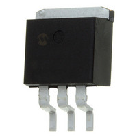
Manufacturer Part Number
MCP1790T-3002E/EB
Description
High Voltage, LDO, 70 MA 3 DDPAK T/R
Manufacturer
Microchip Technology
Datasheet
1.MCP1791T-3302EDC.pdf
(34 pages)
Specifications of MCP1790T-3002E/EB
Regulator Topology
Positive Fixed
Voltage - Output
3V
Voltage - Input
6 ~ 30 V
Voltage - Dropout (typical)
0.7V @ 70mA
Number Of Regulators
1
Current - Output
70mA (Min)
Operating Temperature
-40°C ~ 125°C
Mounting Type
Surface Mount
Package / Case
TO-263-3, D²Pak (3 leads + Tab), TO-263AA
Number Of Outputs
1
Polarity
Positive
Input Voltage Max
30 V
Output Voltage
3 V
Output Type
Fixed
Dropout Voltage (max)
1.3 V at 70 mA
Output Current
70 mA
Line Regulation
+/- 0.0002 % / V
Load Regulation
+/- 0.2 %
Voltage Regulation Accuracy
2.5 %
Maximum Operating Temperature
+ 125 C
Mounting Style
SMD/SMT
Minimum Operating Temperature
- 40 C
Lead Free Status / RoHS Status
Lead free / RoHS Compliant
Current - Limit (min)
-
Lead Free Status / Rohs Status
Lead free / RoHS Compliant
Other names
MCP1790T-3002E/EBTR


AC/DC CHARACTERISTICS (CONTINUED)
© 2008 Microchip Technology Inc.
Electrical Specifications: Unless otherwise noted, V
C
Boldface type applies for junction temperatures, T
Short Circuit Foldback Voltage Corner
Short Circuit Foldback Current
Startup Voltage Overshoot
Dropout Voltage
Dropout Current
I
Shutdown Input
Logic High Input
Logic Low Input
Shutdown Input Leakage Current
Power Good Characteristics
PWRGD Input Voltage Operating
Range
PWRGD Threshold Voltage
(Referenced to V
PWRGD Threshold Hysteresis
PWRGD Output Voltage LOW
PWRGD Output Sink Current
PWRGD Leakage
PWRGD Time Delay
Note 1:
OUT
OUT
= 0 mA
= 4.7 µF (X7R Ceramic), C
2:
3:
4:
5:
6:
7:
8:
9:
The minimum V
V
Load regulation is measured at a constant junction temperature using low duty cycle pulse testing. Load regulation is
tested over a load range from 1 mA to the maximum specified output current.
The maximum allowable power dissipation is a function of ambient temperature, the maximum allowable junction
temperature and the thermal resistance from junction to air. (i.e., T
dissipation will cause the device operating junction temperature to exceed the maximum 165°C rating. Sustained
junction temperatures above 165°C can impact the device reliability.
The junction temperature is approximated by soaking the device under test at an ambient temperature equal to the
desired Junction temperature. The test time is small enough such that the rise in the Junction temperature over the
ambient temperature is not significant.
Dropout voltage is defined as the input-to-output voltage differential at which the output voltage drops 2% below its
nominal value that was measured with an input voltage of V
Sustained junction temperatures above 165°C can impact the device reliability.
The Short Circuit Recovery Time test is done by placing the device into a short circuit condition and then removing the
short circuit condition before the device die temperature reaches 125 °C. If the device goes into thermal shutdown, then
the Short Circuit Recovery Time will depend upon the thermal dissipation properties of the package and circuit board.
TCV
peraturerange. V
Parameters
R
is the nominal regulator output voltage.
OUT
OUT)
= (V
OUT-HIGH
IN
OUT-LOW
, V
IN(MIN)
IN
- V
= 4.7 µF (X7R Ceramic), T
OUT-LOW
= lowest voltage measured over the temperature range.
must meet two conditions: V
V
V
V
V
V
V
I
V
V
PWRGD_HYS
PWRGD
PWRGD_VIN
I
SHDN
SHDN-HIGH
PWRGD_TH
SHDN-LOW
PWRGD_L
Symbol
FOLDBACK
DROPOUT
PWRGD_L
V
T
OVER
I
) *10^6 / (V
DO
PG
ILK
_
J
LK
(Note 5) of -40°C to +125°C.
IN
= V
R
Min
* ΔTemperature), V
OUT(MAX)
2.4
2.8
1.0
5.0
88
—
—
—
—
—
—
—
—
—
—
—
—
—
—
—
—
0
A
= +25°C, SHDN > 2.4V.
IN
+ V
≥ 6.0V and V
0.100
0.10
Typ
105
700
130
4.2
3.0
2.7
3.0
2.0
0.2
1.0
IN
99
99
75
75
90
30
—
—
—
—
DROPOUT(MAX),
= V
MCP1790/MCP1791
R
A
OUT-HIGH
, T
+ V
V
J
, θ
0.500
IN
IN(MAX)
DROPOUT(MAX)
1300
Max
0.8
5.0
3.0
0.4
92
—
—
—
—
—
—
—
—
—
—
—
—
—
—
JA
≥ V
). Exceeding the maximum allowable power
(Note 1), I
= highest voltage measured over the tem-
OUT(MAX)
% V
%V
%V
Units
mA
mA
mA
mV
mA
µA
µA
µA
µA
nA
µs
V
V
V
V
V
V
V
OUT
OUT
OUT
.
OUT
+ V
DROPOUT(MAX).
= 1 mA,
V
Falling V
V
Falling V
V
Falling V
V
R
V
V
V
V
I
V
V
V
SHDN = GND
SHDN = 6V
Falling Edge of V
Rising Edge of V
I
V
V
V
Rising Edge
OUT
PWRGD SINK
R
R
R
OUT
R
R
R
IN
R
R
R
OUT
PWRGD
PWRGD
LOAD
= 5.0V
= 3.3V
= 3.0V
= 5.0V (Note 2)
= 3.3V (Note 2)
= 3.0V (Note 2)
= 5.0V, V
= 3.3V, V
= 3.0V, V
= 0V to 6.0V
= 70 mA, (Note 6)
~= 0V,
= 0V
< 0.1 Ω,
Conditions
OUT,
OUT,
OUT,
<= 0.4V
= V
DS22075A-page 5
IN
IN
IN
IN
= 5.0 mA,
R
R
R
LOAD
LOAD
LOAD
= 4.500V
= 4.500V
= 4.500V
= 6.0V
OUT
OUT
< 0.1 Ω
< 0.1 Ω
< 0.1 Ω
Related parts for MCP1790T-3002E/EB
Image
Part Number
Description
Manufacturer
Datasheet
Request
R

Part Number:
Description:
High Voltage, LDO, 70 MA 3 SOT-223 T/R
Manufacturer:
Microchip Technology
Datasheet:

Part Number:
Description:
High Voltage, LDO, 70 MA 3 DDPAK T/R
Manufacturer:
Microchip Technology
Datasheet:
Part Number:
Description:
High Voltage, LDO, 70 MA 3 DDPAK T/R
Manufacturer:
Microchip Technology
Datasheet:
Part Number:
Description:
High Voltage, LDO, 70 MA 3 SOT-223 T/R
Manufacturer:
Microchip Technology
Datasheet:
Part Number:
Description:
High Voltage, LDO, 70 MA 3 SOT-223 T/R
Manufacturer:
Microchip Technology
Datasheet:
Part Number:
Description:
IC LDO REG 70MA 5.0V SOT-223-3
Manufacturer:
Microchip Technology
Datasheet:
Part Number:
Description:
IC LDO REG 70MA 3.3V 3DDPAK
Manufacturer:
Microchip Technology
Datasheet:
Part Number:
Description:
High Voltage, LDO, 70 MA 3 DDPAK TUBE
Manufacturer:
Microchip Technology
Datasheet:
Part Number:
Description:
IC LDO REG 70MA 3.0V SOT-223-3
Manufacturer:
Microchip Technology
Datasheet:
Part Number:
Description:
IC LDO REG 70MA 3.3V SOT-223-3
Manufacturer:
Microchip Technology
Datasheet:
Part Number:
Description:
IC LDO REG 70MA 3.0V 3DDPAK
Manufacturer:
Microchip Technology
Datasheet:

Part Number:
Description:
High Voltage, LDO, 50 mA, -40C to +125C, 8-SOIC 150mil, TUBE
Manufacturer:
Microchip Technology
Datasheet:

Part Number:
Description:
70 Ma, High Voltage Regulator
Manufacturer:
Microchip Technology Inc.
Datasheet: