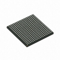
XC6SLX25-2CSG324C Xilinx Inc, XC6SLX25-2CSG324C Datasheet - Page 60

XC6SLX25-2CSG324C
Manufacturer Part Number
XC6SLX25-2CSG324C
Description
FPGA, SPARTAN-6 LX, 24K, 324CSGBGA
Manufacturer
Xilinx Inc
Series
Spartan® 6 LXr
Specifications of XC6SLX25-2CSG324C
No. Of Logic Blocks
3758
No. Of Macrocells
24051
Family Type
Spartan-6
No. Of Speed Grades
2
Total Ram Bits
958464
No. Of I/o's
226
Clock Management
DCM, PLL
I/o Supply Voltage
3.3V
Number Of Logic Elements/cells
24051
Number Of Labs/clbs
1879
Number Of I /o
226
Voltage - Supply
1.14 V ~ 1.26 V
Mounting Type
Surface Mount
Operating Temperature
0°C ~ 85°C
Package / Case
324-LFBGA, CSPBGA
Core Supply Voltage Range
1.14V
Rohs Compliant
Yes
Number Of Gates
-
Lead Free Status / RoHS Status
Lead free / RoHS Compliant
Number Of Gates
-
Lead Free Status / Rohs Status
Lead free / RoHS Compliant
Available stocks
Company
Part Number
Manufacturer
Quantity
Price
Company:
Part Number:
XC6SLX25-2CSG324C
Manufacturer:
Xilinx Inc
Quantity:
10 000
Part Number:
XC6SLX25-2CSG324C
Manufacturer:
XILINX/赛灵思
Quantity:
20 000
Table 65: Global Clock Input to Output Delay With PLL in Source-Synchronous Mode
Table 66: Global Clock Input to Output Delay With DCM and PLL in System-Synchronous Mode
DS162 (v2.0) March 31, 2011
Preliminary Product Specification
Notes:
1.
2.
Notes:
1.
2.
LVCMOS25 Global Clock Input to Output Delay using Output Flip-Flop, 12mA, Fast Slew Rate, with PLL in Source-Synchronous Mode.
T
LVCMOS25 Global Clock Input to Output Delay using Output Flip-Flop, 12mA, Fast Slew Rate, with DCM in System-Synchronous Mode
and PLL in DCM2PLL Mode.
T
ICKOFPLL_0
ICKOFDCM_PLL
Listed above are representative values where one global clock input drives one vertical clock line in each accessible column, and where all accessible
IOB and CLB flip-flops are clocked by the global clock net.
PLL output jitter is included in the timing calculation.
Listed above are representative values where one global clock input drives one vertical clock line in each accessible column, and where all accessible
IOB and CLB flip-flops are clocked by the global clock net.
DCM and PLL output jitter are already included in the timing calculation.
Symbol
Symbol
Global Clock and OUTFF with PLL
Global Clock and OUTFF with DCM and PLL
Description
Description
www.xilinx.com
Spartan-6 FPGA Data Sheet: DC and Switching Characteristics
XC6SLX4
XC6SLX9
XC6SLX16
XC6SLX25
XC6SLX25T
XC6SLX45
XC6SLX45T
XC6SLX75
XC6SLX75T
XC6SLX100
XC6SLX100T
XC6SLX150
XC6SLX150T
XC6SLX4
XC6SLX9
XC6SLX16
XC6SLX25
XC6SLX25T
XC6SLX45
XC6SLX45T
XC6SLX75
XC6SLX75T
XC6SLX100
XC6SLX100T
XC6SLX150
XC6SLX150T
Device
Device
4.78
4.78
4.70
4.70
4.70
4.63
4.63
4.68
4.68
4.72
4.76
4.44
4.44
5.49
5.49
5.23
5.00
5.00
5.59
5.59
4.96
4.96
4.97
5.01
4.59
4.59
-3
-3
6.29
5.77
5.35
5.35
6.03
6.03
5.41
5.41
5.42
5.42
5.06
5.06
5.24
5.12
5.09
5.09
4.98
4.98
5.04
5.04
5.07
5.07
4.73
4.73
Speed Grade
Speed Grade
-3N
N/A
-3N
N/A
6.32
6.32
5.94
5.92
5.92
5.83
5.83
5.88
5.88
5.92
5.92
5.31
5.31
7.44
7.44
6.79
6.10
6.10
7.02
7.02
6.22
6.22
6.21
6.21
5.86
5.86
-2
-2
7.09
7.09
6.63
7.30
7.26
6.90
7.77
6.96
8.55
8.55
8.21
8.54
8.39
8.32
9.08
8.13
N/A
N/A
N/A
N/A
N/A
N/A
N/A
N/A
N/A
N/A
-1L
-1L
Units
Units
ns
ns
ns
ns
ns
ns
ns
ns
ns
ns
ns
ns
ns
ns
ns
ns
ns
ns
ns
ns
ns
ns
ns
ns
ns
ns
60


