W3F11A4718AT3A AVX Corporation, W3F11A4718AT3A Datasheet - Page 2
W3F11A4718AT3A
Manufacturer Part Number
W3F11A4718AT3A
Description
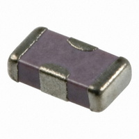
CAP FEEDTHRU 470PF 100V NP0 1206
Manufacturer
AVX Corporation
Series
W3Fr
Datasheet
1.W3F15C2238AT1A.pdf
(4 pages)
Specifications of W3F11A4718AT3A
Capacitance
470pF
Voltage
100V
Current
300mA
Dc Resistance (dcr)
600.0 mOhm
Operating Temperature
-55°C ~ 125°C
Package / Case
1206 (3216 Metric)
Lead Free Status / RoHS Status
Lead free / RoHS Compliant


Feedthru 0805/1206 Capacitors
W2F/W3F Series
DIMENSIONS
RECOMMENDED SOLDER PAD LAYOUT
2
0805 MM
1206 MM
0805 MM
1206 MM
Vcc or
Signal In
The terminals are connected internally side to side.
Left side and right side are connected and front and
back are connected internally.
For Decoupling, the chip is usually surrounded by
four vias, two for Vcc and two for GND.
For Signal Filtering, the in and out lines need to be
separated on the circuit board.
(in.)
(in.)
Feedthru Chip Component Model
(in.)
(in.)
(0.079 ± 0.008)
(0.126 ± 0.008)
2.01 ± 0.20
3.20 ± 0.20
L
Ground
(0.136)
(0.179)
3.45
4.54
T
(0.049 ± 0.008)
(0.063 ± 0.008)
BW
1.25 ± 0.20
1.60 ± 0.20
L
S
W
TYPICAL FEEDTHRU CHIP CAP CONNECTION
X
Vcc or
Signal Out
(0.037)
(0.020)
0.94
0.51
(0.045 Max.)
(0.050 Max.)
P
T
1.14 Max.
1.27 Max.
T
C
P
(0.035 ± 0.004) (0.007 + 0.010 -0.003)
(0.018 ±0.004)
0.46 ± 0.10
0.89 ± 0.10
Common Ground
Feedthru Pad
Common Ground
(0.030)
(0.040)
BW
1.02
T
(TYPICAL DIMENSIONS)
0.76
P
S
Signal In
S
(0.007 + 0.010 -0.003)
Vcc
0.18 + 0.25 -0.08
0.18 + 0.25 -0.08
L
BL
(0.065)
(0.050)
1.65
1.27
Physical Layout - A
Physical Layout - B
W
W
C L
(0.010 ± 0.005)
(0.015 ± 0.007)
Ground
Ground
Ground
Ground
0.25 ± 0.13
0.38 ± 0.18
BL
EW
EW
(0.043)
(0.040)
1.09
1.02
L
W
(0.040 ± 0.004)
(0.063 ± 0.004)
Feedthru Pad
1.02 ± 0.10
1.60 ± 0.10
X
Signal Out
Vcc
(0.009 ± 0.006)
(0.018 ± 0.006)
(0.018)
(0.028)
0.23 ± 0.15
0.46 ± 0.15
0.46
0.71
C
S
Related parts for W3F11A4718AT3A
Image
Part Number
Description
Manufacturer
Datasheet
Request
R

Part Number:
Description:
Manufacturer:
AVX Corporation
Datasheet:
Part Number:
Description:
Manufacturer:
AVX Corporation
Datasheet:
Part Number:
Description:
Manufacturer:
AVX Corporation
Datasheet:
Part Number:
Description:
Manufacturer:
AVX Corporation
Datasheet:
Part Number:
Description:
Manufacturer:
AVX Corporation
Datasheet: