SY89837UMI TR Micrel Inc, SY89837UMI TR Datasheet - Page 3
SY89837UMI TR
Manufacturer Part Number
SY89837UMI TR
Description
Manufacturer
Micrel Inc
Type
Clock Driverr
Datasheet
1.SY89837UMI_TR.pdf
(14 pages)
Specifications of SY89837UMI TR
Number Of Clock Inputs
2
Mode Of Operation
Differential
Output Frequency
2000MHz
Output Logic Level
LVPECL
Operating Supply Voltage (min)
2.375V
Operating Supply Voltage (typ)
2.5/3.3V
Operating Supply Voltage (max)
3.6V
Package Type
MLF
Operating Temp Range
-40C to 85C
Operating Temperature Classification
Industrial
Signal Type
CML/LVDS/PECL
Mounting
Surface Mount
Pin Count
32
Lead Free Status / RoHS Status
Not Compliant


M9999-060410
hbwhelp@micrel.com or (408) 955-1690
Micrel, Inc.
9, 19, 22, 32
30, 28, 26, 24,
18, 16, 14, 12,
29, 27, 25, 23,
17, 15, 13, 11
PACKAGE/ORDERING INFORMATION
Pin Number
PIN DESCRIPTION
20,21
1, 3,
6, 8
2, 7
4,5
31
10
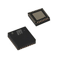
32-Pin MLF
Exposed Pad
VREF-AC0
VREF-AC1
Pin Name
IN0, /IN0,
VT0, VT1
/Q0 – /Q7
IN1, /IN1
Q0 – Q7,
®
GND,
VCC
CAP
SEL
(MLF-32)
Pin Function
Differential Inputs: These input pairs are the differential signal inputs to the device. These inputs
accept AC- or DC-coupled signals as small as 200mV. Each pin of a pair internally terminates to
a VT pin through 50Ω. Please refer to the “Input Interface Applications” section for more details.
Input Termination Center-Tap: Each side of the differential input pair terminates to a VT pin. The
VT0 and VT1 pins provide a center-tap to a termination network for maximum interface flexibility.
See the “Input Interface Applications” section for more details.
This single-ended TTL/CMOS-compatible input selects the inputs to the multiplexer. This input
is internally connected to a 25kΩ pull-up resistor and will default to a logic HIGH state if left open.
Positive power supply. Bypass with 0.1µF
possible.
Differential Outputs: These LVPECL output pairs are the outputs of the device. They are a logic
function of the IN0, IN1, and SEL inputs. Please refer to the truth table for details. Unused
output pairs may be left open.
Ground. Ground and exposed pad to be tied together to most negative potential of chip.
Power-On Reset (POR) Initialization Capacitor. When using the multiplexer with RPE capability,
this pin is tied to a capacitor to V
a known state. If this pin is tied to V
function as a normal multiplexer. See “Application” section for more details. The CAP pin should
never be left open.
Reference Voltage: These outputs bias to V
(IN,/IN). Connect VREF_AC directly to the VT pin. Bypass with 0.01µF low ESR capacitor to
VCC. See "Input Interface Applications" section. Maximum sink/source current is ±1.5mA.
Ordering Information
Notes:
1. Contact factory for die availability. Dice are guaranteed at T
2. Tape and Reel.
3. Pb-Free package is recommended for new designs.
Part Number
SY89837UMI
SY89837UMITR
SY89837UMG
SY89837UMGTR
(3)
(2)
(2, 3)
3
CC
. The purpose is to ensure the internal RPE logic starts up in
CC
Package
MLF-32
MLF-32
MLF-32
MLF-32
, the RPE function will be disabled and the multiplexer will
Type
CC
0.01µF low ESR capacitors as close to the pins as
(1)
- 1.2V. They are used for AC-coupling inputs
Operating
Industrial
Industrial
Industrial
Industrial
Range
Pb-Free bar-line indicator
Pb-Free bar-line indicator
SY89837U with
SY89837U with
A
= 25°C, DC Electricals only.
SY89837U
SY89837U
Package
Marking
Precision Edge
SY89837U
Pb-Free
Pb-Free
NiduAu
NiduAu
Finish
Sn-Pb
Sn-Pb
Lead
®
Related parts for SY89837UMI TR
Image
Part Number
Description
Manufacturer
Datasheet
Request
R

Part Number:
Description:
Manufacturer:
Micrel Inc
Datasheet:
Part Number:
Description:
Manufacturer:
Micrel Inc
Datasheet:
Part Number:
Description:
Manufacturer:
Micrel Inc
Datasheet:
Part Number:
Description:
Manufacturer:
Micrel Inc
Datasheet:
Part Number:
Description:
Manufacturer:
Micrel Inc
Datasheet:
Part Number:
Description:
Manufacturer:
Micrel Inc
Datasheet:
Part Number:
Description:
Manufacturer:
Micrel Inc
Datasheet:
Part Number:
Description:
Manufacturer:
Micrel Inc
Datasheet:
Part Number:
Description:
Manufacturer:
Micrel Inc
Datasheet:
Part Number:
Description:
Manufacturer:
Micrel Inc
Datasheet:
Part Number:
Description:
Manufacturer:
Micrel Inc
Datasheet:
Part Number:
Description:
Manufacturer:
Micrel Inc
Datasheet:
Part Number:
Description:
Manufacturer:
Micrel Inc
Datasheet:
Part Number:
Description:
Manufacturer:
Micrel Inc
Datasheet: