CY29947AC Cypress Semiconductor Corp, CY29947AC Datasheet
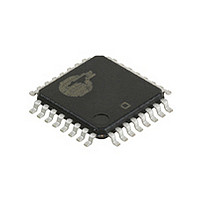
CY29947AC

Manufacturer Part Number
CY29947AC
Description
Manufacturer
Cypress Semiconductor Corp
Type
Clock Driverr
Datasheet

Specifications of CY29947AC

Number Of Clock Inputs
2
Mode Of Operation
Single-Ended
Output Frequency
200MHz
Output Logic Level
LVCMOS/LVTTL
Operating Supply Voltage (min)
2.375V
Operating Supply Voltage (typ)
2.5/3.3V
Operating Supply Voltage (max)
3.63V
Package Type
TQFP
Operating Temp Range
0C to 70C
Operating Temperature Classification
Commercial
Signal Type
LVCMOS/LVTTL
Mounting
Surface Mount
Pin Count
32
Quiescent Current
7mA
Lead Free Status / RoHS Status
Not Compliant

Available stocks

Company
Part Number
Manufacturer
Quantity
Price
Part Number:
CY29947AC
Manufacturer:
CY
Quantity:
1 376
47
Features
Cypress Semiconductor Corporation
Document #: 38-07287 Rev. *C
• 2.5V or 3.3V operation
• 200-MHz clock support
• LVCMOS-/LVTTL-compatible inputs
• 9 clock outputs: drive up to 18 clock lines
• Synchronous Output Enable
• Output three-state control
• 250 ps max. output-to-output skew
• Pin compatible with MPC947, MPC9447
• Available in Industrial and Commercial temp. range
• 32-pin TQFP package
Block Diagram
TCLK_SEL
SYNC_OE
TCLK0
TCLK1
TS#
0
1
VDD
VDDC
2.5V or 3.3V, 200-MHz, 1:9 Clock Distribution Buffer
3901 North First Street
9
Q0-Q8
Description
The CY29947 is a low-voltage 200-MHz clock distribution buff-
er with the capability to select one of two LVCMOS/LVTTL
compatible clock inputs. The two clock sources can be used
to provide for a test clock as well as the primary system clock.
All other control inputs are LVCMOS/LVTTL compatible. The 9
outputs are LVCMOS or LVTTL compatible and can drive 50
series or parallel terminated transmission lines.For series ter-
minated transmission lines, each output can drive one or two
traces giving the device an effective fanout of 1:18. The out-
puts can also be three-stated via the three-state input TS#.
Low output-to-output skews make the CY29947 an ideal clock
distribution buffer for nested clock trees in the most demand-
ing of synchronous systems.
The CY29947 also provides a synchronous output enable in-
put for enabling or disabling the output clocks. Since this input
is internally synchronized to the input clock, potential output
glitching or runt pulse generation is eliminated.
Pin Configuration
TCLK_SEL
SYNC_OE
TCLK0
TCLK1
VDD
VSS
VSS
TS#
San Jose
1
2
3
4
5
6
7
8
CY29947
CA 95134
Revised December 22, 2002
24
23
22
21
20
19
18
17
VSS
Q3
VDDC
Q4
VSS
Q5
VDDC
VSS
CY29947
408-943-2600
[+] Feedback

Related parts for CY29947AC

CY29947AC Summary of contents

Page 1

... TCLK1 TCLK_SEL SYNC_OE TS# Cypress Semiconductor Corporation Document #: 38-07287 Rev. *C 2.5V or 3.3V, 200-MHz, 1:9 Clock Distribution Buffer Description The CY29947 is a low-voltage 200-MHz clock distribution buff- er with the capability to select one of two LVCMOS/LVTTL compatible clock inputs. The two clock sources can be used to provide for a test clock as well as the primary system clock ...

Page 2

Pin Description Pin Name PWR 3 TCLK0 4 TCLK1 2 TCLK_SEL 11, 13, 15, 19, Q(8:0) VDDC 21, 23, 26, 28 SYNC_OE 6 TS# 10, 14, 18, 22, VDDC 27 VDD 12, ...

Page 3

Maximum Ratings Maximum Input Voltage Relative ............. V SS Maximum Input Voltage Relative to V :............. V DD Storage Temperature: ................................ –65° 150°C Operating Temperature: ................................ –40°C to +85°C Maximum ESD protection ................................................ 2kV ...

Page 4

AC Parameters : 3.3V ±10% or 2.5V ±5%, Over the specified temperature range DD DDC Parameter Description [6] Fmax Input Frequency [6] Tpd TCLK To Q Delay [6, 7] FoutDC Output Duty Cycle tpZL, tpZH ...

Page 5

Pulse Generator ohm Figure 2. LVCMOS_CLK CY29947 Test Reference for V LVCMOS_CLK Q Figure 3. LVCMOS Propagation Delay (TPD) Test Reference Document #: 38-07287 Rev. *C CY29947 DUT ohm ohm R ...

Page 6

... Pin TQFP CY29947AIT 32 Pin TQFP - Tape and Reel CY29947AC 32 Pin TQFP CY29947ACT 32 Pin TQFP - Tape and Reel Package Drawing and Dimensions 32-Lead Thin Plastic Quad Flatpack 1.0mm A32 All product and company names mentioned in this document may be the trademarks of their respective holders. ...

Page 7

Revision History Document Title: CY29947 2.5V or 3.3V, 200-MHz, 1:9 Clock Distribution Buffer Document Number: 38-07287 Issue REV. ECN NO. Date Change ** 111098 02/07/02 *A 116781 08/14/02 *B 118462 09/09/02 *C 122879 12/22/02 Document #: 38-07287 Rev. *C Orig. ...

Related keywords