MMBV105GLT1G ON Semiconductor, MMBV105GLT1G Datasheet

DIODE TUNING SS 30V SOT23

MMBV105GLT1G

Manufacturer Part Number
MMBV105GLT1G
Description
DIODE TUNING SS 30V SOT23
Manufacturer
ON Semiconductor
Datasheets

Specifications of MMBV105GLT1G

Capacitance @ Vr, F
2.8pF @ 25V, 1MHz
Capacitance Ratio
6.5
Capacitance Ratio Condition
C3/C25
Voltage - Peak Reverse (max)
30V
Diode Type
Single
Q @ Vr, F
250 @ 3V, 50MHz
Mounting Type
Surface Mount
Package / Case
SOT-23-3, TO-236-3, Micro3™, SSD3, SST3
Capacitance, Junction
2.8 pF
Current, Forward
200 mA
Package Type
SOT-23 (TO-236)
Power Dissipation
225 mW
Primary Type
Tuning
Temperature, Junction, Maximum
+125 °C
Voltage, Reverse
30 V
Capacitance Cd Max @ Vr F
2.8pF
Q @ Vr F
250
Forward Current If(av)
200mA
Repetitive Reverse Voltage Vrrm Max
30V
Diode Case Style
SOT-23
No. Of Pins
3
Capacitance Ratio Min, Cvr1/cvr2
4
Rohs Compliant
Yes
Current Rating
200mA
Lead Free Status / RoHS Status
Lead free / RoHS Compliant
Other names
MMBV105GLT1GOS
MMBV105GLT1GOS
MMBV105GLT1GOSTR

Available stocks

Company
Part Number
Manufacturer
Quantity
Price
Part Number:
MMBV105GLT1G
Manufacturer:
ON Semiconductor
Quantity:
2 800
Part Number:
MMBV105GLT1G
Manufacturer:
ON
Quantity:
30 000
Part Number:
MMBV105GLT1G
Manufacturer:
ON/安森美
Quantity:
20 000
MMBV105GLT1
Silicon Tuning Diode
frequency control and tuning applications. It provides solid−state
reliability in replacement of mechanical tuning methods.
Features
Maximum ratings are those values beyond which device damage can occur.
Maximum ratings applied to the device are individual stress limit values (not
normal operating conditions) and are not valid simultaneously. If these limits are
exceeded, device functional operation is not implied, damage may occur and
reliability may be affected.
© Semiconductor Components Industries, LLC, 2006
MAXIMUM RATINGS
Reverse Voltage
Forward Current
Device Dissipation @ T
Junction Temperature
Storage Temperature Range
This device is designed in the Surface Mount package for general
Controlled and Uniform Tuning Ratio
Pb−Free Package is Available
Derate above 25°C
Rating
A
(T
= 25°C
C
= 25°C unless otherwise noted)
Preferred Device
Symbol
T
V
P
T
I
stg
F
R
D
J
−55 to +150
Value
+125
200
225
1.8
30
1
mW/°C
mAdc
Unit
Vdc
mW
°C
°C
†For information on tape and reel specifications,
MMBV105GLT1
MMBV105GLT1G
Preferred devices are recommended choices for future use
and best overall value.
including part orientation and tape sizes, please
refer to our Tape and Reel Packaging Specifications
Brochure, BRD8011/D.
*Date Code orientation and/or overbar may
Device
vary depending upon manufacturing location.
(Note: Microdot may be in either location)
ORDERING INFORMATION
M4E = Specific Device Code
M
G
Cathode
MARKING DIAGRAM
3
SOT−23 (TO−236)
= Date Code*
= Pb−Free Package
1
1
(Pb−Free)
Package
CASE 318
SOT−23
SOT−23
STYLE 8
M4EM G
2
G
3
3,000 / Tape & Reel
3,000 / Tape & Reel
Anode
1
Shipping

Related parts for MMBV105GLT1G

MMBV105GLT1G Summary of contents

Page 1

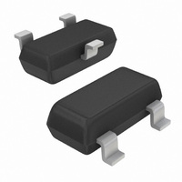
... ORDERING INFORMATION Device Package Shipping MMBV105GLT1 SOT−23 3,000 / Tape & Reel MMBV105GLT1G SOT−23 3,000 / Tape & Reel (Pb−Free) †For information on tape and reel specifications, including part orientation and tape sizes, please refer to our Tape and Reel Packaging Specifications Brochure, BRD8011/D. ...

Page 2

ELECTRICAL CHARACTERISTICS Characteristic Reverse Breakdown Voltage = 10 mAdc Reverse Voltage Leakage Current ( Vdc) R Device Type MMBV105GLT1 8.0 6 1.0 MHz T = 25°C A 4.0 ...

Page 3

... *For additional information on our Pb−Free strategy and soldering details, please download the ON Semiconductor Soldering and Mounting Techniques Reference Manual, SOLDERRM/D. MMBV105GLT1 PACKAGE DIMENSIONS SOT−23 (TO−236) CASE 318−08 ISSUE AN NOTES: 1. DIMENSIONING AND TOLERANCING PER ANSI Y14.5M, 1982. 2. CONTROLLING DIMENSION: INCH. ...

Related keywords