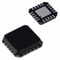
ADG788BCPZ Analog Devices Inc, ADG788BCPZ Datasheet - Page 3

ADG788BCPZ
Manufacturer Part Number
ADG788BCPZ
Description
Analog Switch Quad SPDT 20-Pin LFCSP EP
Manufacturer
Analog Devices Inc
Type
Analog Switchr
Datasheet
1.ADG788BCPZ.pdf
(12 pages)
Specifications of ADG788BCPZ
Function
Switch
Circuit
4 x SPDT
On-state Resistance
4.5 Ohm
Voltage Supply Source
Single, Dual Supply
Voltage - Supply, Single/dual (±)
1.8 V ~ 5.5 V, ±2.5 V
Current - Supply
0.001µA
Operating Temperature
-40°C ~ 85°C
Mounting Type
Surface Mount
Package / Case
20-VFQFN, CSP Exposed Pad
Package/case
20-CSP
Leakage Current
100nA
On-resistance, Rds(on)
2.5mOhm
Number Of Circuits
4
Rohs Compliant
Yes
No. Of Channels
4
Bandwidth
160MHz
On State Resistance Max
5ohm
Turn Off Time
7ns
Turn On Time
19ns
Supply Voltage Range
1.8V To 5.5V
Operating Temperature Range
-40°C To +85°C
Multiplexer Configuration
Quad SPDT
Number Of Inputs
4
Number Of Outputs
8
Number Of Channels
4
Analog Switch On Resistance
11@3VOhm
Analog Switch Turn On Time
28ns
Analog Switch Turn Off Time
10ns
Package Type
LFCSP
Power Supply Requirement
Single/Dual
Single Supply Voltage (min)
1.8V
Single Supply Voltage (typ)
3/5V
Single Supply Voltage (max)
5.5V
Dual Supply Voltage (typ)
±2.5V
Power Dissipation
0.000005W
Supply Current
0.001mA
Mounting
Surface Mount
Pin Count
20
Operating Temp Range
-40C to 85C
Operating Temperature Classification
Industrial
Lead Free Status / RoHS Status
Lead free / RoHS Compliant
For Use With
EVAL-ADG788EBZ - BOARD EVALUATION FOR ADG788
Lead Free Status / Rohs Status
Compliant
Available stocks
Company
Part Number
Manufacturer
Quantity
Price
Company:
Part Number:
ADG788BCPZ
Manufacturer:
ADI
Quantity:
218
Part Number:
ADG788BCPZ
Manufacturer:
ADI/亚德诺
Quantity:
20 000
SPECIFICATIONS
Parameter
LEAKAGE CURRENTS
DIGITAL INPUTS
DYNAMIC CHARACTERISTICS
POWER REQUIREMENTS
NOTES
1
2
Specifications subject to change without notice.
ANALOG SWITCH
Temperature ranges are as follows: B Version: –40 C to +85 C.
Guaranteed by design, not subject to production test.
Analog Signal Range
On Resistance (R
On-Resistance Match between
On-Resistance Flatness (R
Source OFF Leakage I
Channel ON Leakage I
Input High Voltage, V
Input Low Voltage, V
Input Current
C
t
t
ADG786 t
Break-Before-Make Time Delay, t
Charge Injection
Off Isolation
Channel-to-Channel Crosstalk
–3 dB Bandwidth
C
C
I
ON
OFF
DD
IN
S
D
Channels ( R
I
, C
INL
(OFF)
, Digital Input Capacitance
S
or I
(ON)
INH
t
ON
OFF
(EN)
(EN)
ON
ON
)
)
INL
INH
S
D
(OFF)
, I
FLAT(ON)
S
(ON)
1
(V
2
D
)
DD
= 3 V
+25 C
6
11
0.005
4
28
9
29
9
22
–72
–67
160
11
34
0.001
0.01
0.1
0.01
0.1
3
10%, V
B Version
SS
= 0 V, GND = 0 V, unless otherwise noted.)
–40 C
to +85 C
0 V to V
12
0.1
0.5
3
55
16
60
16
1
1.0
2.0
0.8
0.3
0.5
0.1
DD
Unit
V
nA typ
nA max
nA typ
nA max
V min
V max
pF typ
ns typ
ns max
ns typ
ns max
ns typ
ns max
ns typ
ns max
ns typ
ns min
pC typ
dB typ
dB typ
MHz typ
pF typ
pF typ
A typ
A max
A typ
A max
typ
max
typ
max
typ
Test Conditions/Comments
V
Test Circuit 1
V
V
V
V
Test Circuit 2
V
Test Circuit 3
V
R
V
R
V
R
V
R
V
R
V
V
Test Circuit 7
R
Test Circuit 8
R
Test Circuit 9
R
f = 1 MHz
f = 1 MHz
V
Digital Inputs = 0 V or 3.3 V
S
S
S
DD
S
S
IN
L
S1A
L
S
L
S
L
S
L
S
S
L
L
L
DD
= 0 V to V
= 0 V to V
= 0 V to V
= 3 V/1 V, V
= V
= 2 V, Test Circuit 4
= 2 V, Test Circuit 5
= 2 V, Test Circuit 5
= 2 V, Test Circuit 6
= 1 V, R
= 300 , C
= 300 , C
= 300 , C
= 300 , C
= 300 , C
= 50 , C
= 50 , C
= 50 , C
= V
= 3.3 V
= 3.3 V
= 2 V, V
D
INL
= 1 V or 3 V;
or V
S
= 0 , C
L
L
L
DD
DD
DD
S1B
L
L
L
L
L
= 5 pF, f = 1 MHz;
= 5 pF, f = 1 MHz;
= 5 pF, Test Circuit 10
INH
D
, I
, I
, I
= 35 pF;
= 35 pF;
= 35 pF;
= 35 pF;
= 35 pF;
= 0 V, Test Circuit 4
ADG786/ADG788
= 1 V/3 V;
DS
DS
DS
= 10 mA;
= 10 mA
= 10 mA
L
= 1 nF;


