DTC123YUAT106 Rohm Semiconductor, DTC123YUAT106 Datasheet - Page 2
DTC123YUAT106
Manufacturer Part Number
DTC123YUAT106
Description
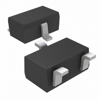
TRANS NPN 50V 100MA SOT-323
Manufacturer
Rohm Semiconductor
Datasheet
1.DTC123YKAT146.pdf
(3 pages)
Specifications of DTC123YUAT106
Transistor Type
NPN - Pre-Biased
Current - Collector (ic) (max)
100mA
Voltage - Collector Emitter Breakdown (max)
50V
Resistor - Base (r1) (ohms)
2.2K
Resistor - Emitter Base (r2) (ohms)
10K
Dc Current Gain (hfe) (min) @ Ic, Vce
33 @ 10mA, 5V
Vce Saturation (max) @ Ib, Ic
300mV @ 500µA, 10mA
Frequency - Transition
250MHz
Power - Max
200mW
Mounting Type
Surface Mount
Package / Case
SC-70, SOT-323
Digital
UMT
Collector Emitter Voltage V(br)ceo
50V
Power Dissipation Pd
200mW
Dc Collector Current
100mA
Operating Temperature Range
-55°C To +150°C
Transistor Case Style
SOT-323
No. Of
RoHS Compliant
Transistor Polarity
NPN
Dc Current Gain Hfe
33
Rohs Compliant
Yes
Lead Free Status / RoHS Status
Lead free / RoHS Compliant
Other names
DTC123YUAT106
DTC123YUAT106TR
DTC123YUAT106TR


Electrical characteristics (Ta=25C)
Electrical characteristic curves
○
DTC123YE / DTC123YUA / DTC123YKA
Characteristics of built-in transistor
c
www.rohm.com
Input voltage
Output voltage
Input current
Output current
DC current gain
Input resistance
Resistance ratio
Transition frequency
Fig.1
500m
200m
100m
500m
200m
100m
50m
20m
10m
2009 ROHM Co., Ltd. All rights reserved.
100
5m
2m
1m
50
20
10
100 200
100 200
5
2
1
1
Fig.4
Parameter
(ON characteristics)
Input voltage vs. output current
OUTPUT CURRENT : I
OUTPUT CURRENT : I
500 1m
500 1m
Output voltage vs. output
current
Ta100°C
40°C
Ta40°C
25°C
2m
2m
100°C
25°C
5m 10m 20m 50m 100m
5m 10m 20m
O
O
Symbol
R
(A)
(A)
V
V
V
I
O(off)
V
l
O(on)
G
R
2
O
I(off)
I(on)
f
I
/R
O
T
I
/l
1
0.3V
I
I
20
1
50m 100m
Min.
1.54
3.6
33
3
Typ.
250
0.1
2.2
4.5
Max.
2.86
0.3
0.3
3.8
0.5
5.5
Fig.2
500
200
100
10m
50
20
10
5m
2m
1m
5
2
1
0
MHz
Unit
mA
A
k
V
V
Output current vs. input voltage
(OFF characteristics)
0.5
INPUT VOLTAGE : V
V
V
I
V
V
V
V
O
CC
O
I
CC
O
CE
/I
5V
0.3V, I
5V, I
1.0
I
10mA/0.5mA
5V, I
50V, V
10V, I
Ta100°C
2/2
O
40°C
1.5
10mA
25°C
O
E
Conditions
O
100A
I
5mA, f100MHz
0V
20mA
2.0
I (off)
(V)
V
2.5
CC
5V
3.0
500
200
100
50
20
10
1k
5
2
1
100 200
Fig.3
OUTPUT CURRENT : I
500 1m
current
DC current gain vs. output
Ta100°C
2009.06 - Rev.B
40°C
25°C
2m
Data Sheet
5m 10m 20m
O
(A)
V
O
5V
50m 100m
Related parts for DTC123YUAT106
Image
Part Number
Description
Manufacturer
Datasheet
Request
R

Part Number:
Description:
12A Bidirectional Thyristor
Manufacturer:
Sanyo Semicon Device
Datasheet:

Part Number:
Description:
Manufacturer:
Rohm Semiconductor
Datasheet:
Part Number:
Description:
Manufacturer:
Rohm Semiconductor
Datasheet:
Part Number:
Description:
Manufacturer:
Rohm Semiconductor
Datasheet:
Part Number:
Description:
Manufacturer:
Rohm Semiconductor
Datasheet:
Part Number:
Description:
Manufacturer:
Rohm Semiconductor
Datasheet:
Part Number:
Description:
Manufacturer:
Rohm Semiconductor
Datasheet:
Part Number:
Description:
Manufacturer:
Rohm Semiconductor
Datasheet:
Part Number:
Description:
Manufacturer:
Rohm Semiconductor
Datasheet:
Part Number:
Description:
Manufacturer:
Rohm Semiconductor
Datasheet:
Part Number:
Description:
Manufacturer:
Rohm Semiconductor
Datasheet:
Part Number:
Description:
Manufacturer:
Rohm Semiconductor
Datasheet:
Part Number:
Description:
Manufacturer:
Rohm Semiconductor
Datasheet: