MJD3055 ON Semiconductor, MJD3055 Datasheet

TRANS POWER NPN 10A 60V DPAK

MJD3055

Manufacturer Part Number
MJD3055
Description
TRANS POWER NPN 10A 60V DPAK
Manufacturer
ON Semiconductor
Datasheet

Specifications of MJD3055

Transistor Type
NPN
Current - Collector (ic) (max)
10A
Voltage - Collector Emitter Breakdown (max)
60V
Vce Saturation (max) @ Ib, Ic
8V @ 3.3A, 10A
Current - Collector Cutoff (max)
50µA
Dc Current Gain (hfe) (min) @ Ic, Vce
20 @ 4A, 4V
Power - Max
1.75W
Frequency - Transition
2MHz
Mounting Type
Surface Mount
Package / Case
DPak, TO-252 (2 leads+tab), SC-63
Lead Free Status / RoHS Status
Contains lead / RoHS non-compliant

Available stocks

Company
Part Number
Manufacturer
Quantity
Price
Part Number:
MJD3055
Manufacturer:
ST
0
Part Number:
MJD3055
Manufacturer:
ON/安森美
Quantity:
20 000
Part Number:
MJD3055G
Manufacturer:
ON
Quantity:
12 500
Part Number:
MJD3055G
Manufacturer:
ON/安森美
Quantity:
20 000
Part Number:
MJD3055T4
Manufacturer:
ON
Quantity:
14 085
Part Number:
MJD3055T4
Manufacturer:
COOPER
Quantity:
1 000
Part Number:
MJD3055T4
Manufacturer:
ST
0
Company:
Part Number:
MJD3055T4
Quantity:
9 000
Company:
Part Number:
MJD3055T4
Quantity:
9 000
Part Number:
MJD3055T4G
Manufacturer:
ON Semiconductor
Quantity:
1
Part Number:
MJD3055T4G
Manufacturer:
ON
Quantity:
12 500
Part Number:
MJD3055T4G
Manufacturer:
ST
0
Part Number:
MJD3055T4G
Manufacturer:
ON/安森美
Quantity:
20 000
Part Number:
MJD3055T4G
0
Company:
Part Number:
MJD3055T4G
Quantity:
100
Company:
Part Number:
MJD3055T4G
Quantity:
2 500
Part Number:
MJD3055TF
Manufacturer:
FAIRCHILD/仙童
Quantity:
20 000
MJD2955 (PNP)
MJD3055 (NPN)
Complementary Power
Transistors
DPAK For Surface Mount Applications
applications.
Features
Stresses exceeding Maximum Ratings may damage the device. Maximum
Ratings are stress ratings only. Functional operation above the Recommended
Operating Conditions is not implied. Extended exposure to stresses above the
Recommended Operating Conditions may affect device reliability.
†Safe Area Curves are indicated by Figure 1. Both limits are applicable and must
1. These ratings are applicable when surface mounted on the minimum pad
© Semiconductor Components Industries, LLC, 2011
January, 2011 − Rev. 10
MAXIMUM RATINGS
THERMAL CHARACTERISTICS
Collector−Emitter Voltage
Collector−Base Voltage
Emitter−Base Voltage
Collector Current
Base Current
Total Power Dissipation @ T
Derate above 25°C
Total Power Dissipation (Note1)
Operating and Storage Junction
Temperature Range
Thermal Resistance, Junction−to−Case
Thermal Resistance, Junction−to−Ambient
(Note1)
be observed.
Designed for general purpose amplifier and low speed switching
(No Suffix)
Lead Formed for Surface Mount Applications in Plastic Sleeves
Straight Lead Version in Plastic Sleeves (“−1” Suffix)
Electrically Similar to MJE2955 and MJE3055
DC Current Gain Specified to 10 Amperes
High Current Gain−Bandwidth Product − f
Epoxy Meets UL 94 V−0 @ 0.125 in
ESD Ratings: Human Body Model, 3B u 8000 V
These are Pb−Free Packages
sizes recommended.
@ T
Derate above 25°C
Characteristic
A
= 25°C
Rating
Machine Model, C u 400 V
C
= 25°C
Symbol
Symbol
T
V
R
R
J
P
V
V
P
CEO
, T
I
I
qJC
qJA
CB
EB
D
C
B
D
T
{
stg
= 2.0 MHz (Min) @ I
= 500 mAdc
−55 to +150
0.014
Max
0.16
1.75
Max
6.25
71.4
60
70
10
20
5
6
1
W/°C
W/°C
°C/W
°C/W
Unit
Unit
Vdc
Vdc
Vdc
Adc
Adc
°C
W
W
C
See detailed ordering and shipping information in the package
dimensions section on page 2 of this data sheet.
1 2
1
POWER TRANSISTORS
2
60 VOLTS, 20 WATTS
3
3
ORDERING INFORMATION
A
Y
WW
Jxx55 = Device Code
G
http://onsemi.com
4
10 AMPERES
4
CASE 369C
CASE 369D
STYLE 1
STYLE 1
DPAK−3
SILICON
= Assembly Location
= Year
= Work Week
= Pb−Free Package
DPAK
x = 29 or 30
Publication Order Number:
DIAGRAMS
MARKING
AYWW
xx55G
AYWW
xx55G
J
MJD2955/D
J

Related parts for MJD3055

MJD3055 Summary of contents

Page 1

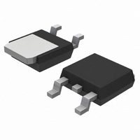
... MJD2955 (PNP) MJD3055 (NPN) Complementary Power Transistors DPAK For Surface Mount Applications Designed for general purpose amplifier and low speed switching applications. Features • Lead Formed for Surface Mount Applications in Plastic Sleeves (No Suffix) • Straight Lead Version in Plastic Sleeves (“−1” Suffix) • ...

Page 2

... Pulse Test: Pulse Width v 300 ms, Duty Cycle v 2%. ORDERING INFORMATION Device MJD2955G MJD2955−1G MJD2955T4G MJD3055G MJD3055T4G †For information on tape and reel specifications, including part orientation and tape sizes, please refer to our Tape and Reel Packaging Specifications Brochure, BRD8011/ 25_C unless otherwise noted) C Characteristic ...

Page 3

... Figure 2. DC Current Gain 1.4 1 25° 0.8 BE(sat 0 0.4 0 CE(sat 0.1 0.2 0.3 0 COLLECTOR CURRENT (AMP) C Figure 4. “On” Voltages, MJD3055 TYPICAL CHARACTERISTICS SURFACE MOUNT 50 75 100 125 T, TEMPERATURE (°C) Figure 1. Power Derating 0.7 0.5 0.3 0.2 0.1 0.07 0.05 0.03 0. 0.06 0 0.7 ...

Page 4

T = 25°C J 1.6 1 BE(sat 0 0 CE(sat 0.1 0.2 0.3 0.5 ...

Page 5

... DETAIL 0.005 (0.13 0.228 *For additional information on our Pb−Free strategy and soldering details, please download the ON Semiconductor Soldering and Mounting Techniques Reference Manual, SOLDERRM/D. PACKAGE DIMENSIONS DPAK CASE 369C−01 ISSUE GAUGE L2 SEATING C PLANE PLANE DETAIL A ROTATED SOLDERING FOOTPRINT* 6.20 3.0 ...

Page 6

... Opportunity/Affirmative Action Employer. This literature is subject to all applicable copyright laws and is not for resale in any manner. PUBLICATION ORDERING INFORMATION LITERATURE FULFILLMENT: Literature Distribution Center for ON Semiconductor P.O. Box 5163, Denver, Colorado 80217 USA Phone: 303−675−2175 or 800−344−3860 Toll Free USA/Canada Fax: 303− ...

Related keywords