2SA1162GT1 ON Semiconductor, 2SA1162GT1 Datasheet
2SA1162GT1
Specifications of 2SA1162GT1


Related parts for 2SA1162GT1

2SA1162GT1 Summary of contents
Page 1
... General Purpose Amplifier Transistors PNP Surface Mount Moisture Sensitivity Level: 1 ESD Rating: TBD MAXIMUM RATINGS ( Rating Symbol Collector−Base Voltage V (BR)CBO Collector−Emitter Voltage V (BR)CEO Emitter−Base Voltage V (BR)EBO Collector Current − Continuous Collector Current − Peak Base Current ...
Page 2
... I C SMALL−SIGNAL CHARACTERISTICS Current −Gain − Bandwidth Product (I = 1 MHz Output Capacitance ( 1.0 MHz) CB Noise Figure (I = 0.1 mA 6.0 Vdc kW 1.0 kHz 200 Hz 300 ms, D.C. 1. Pulse Test: Pulse Width 2SA1162GT1, 2SA1162YT1 ( unless otherwise noted) A Symbol = (BR)CEO = (BR)CBO = (BR)EBO = CBO I EBO ...
Page 3
... When us- ing infrared heating with the reflow soldering method, the difference should be a maximum 2SA1162GT1, 2SA1162YT1 interface between the board and the package. With the correct pad geometry, the packages will self align when subjected to a solder reflow process. ...
Page 4
... DESIRED CURVE FOR HIGH MASS ASSEMBLIES 150 C 100 TIME ( MINUTES TOTAL) 2SA1162GT1, 2SA1162YT1 SOLDER STENCIL GUIDELINES The stencil opening size for the surface mounted package should be the same as the pad size on the printed circuit board, i.e., a 1:1 registration. TYPICAL SOLDER HEATING PROFILE ...
Page 5
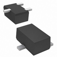
... PACKAGE DIMENSIONS CASE 318D− http://onsemi.com SC−59 ISSUE F NOTES: 1. DIMENSIONING AND TOLERANCING PER ANSI Y14.5M, 1982. 2. CONTROLLING DIMENSION: MILLIMETER. MILLIMETERS DIM MIN MAX A 2.70 3.10 0.1063 B 1.30 1.70 0.0512 C 1.00 1.30 0.0394 D 0.35 0.50 0.0138 G 1.70 2.10 0.0670 H 0 ...
Page 6
... P.O. Box 5163, Denver, Colorado 80217 USA Phone: 303−675−2175 or 800−344−3860 Toll Free USA/Canada Fax: 303−675−2176 or 800−344−3867 Toll Free USA/Canada Email: orderlit@onsemi.com 2SA1162GT1, 2SA1162YT1 N. American Technical Support: 800−282−9855 Toll Free USA/Canada Japan: ON Semiconductor, Japan Customer Focus Center 2− ...