MJE13003 ON Semiconductor, MJE13003 Datasheet

TRANS PWR NPN 1.5A 400V TO225

MJE13003

Manufacturer Part Number
MJE13003
Description
TRANS PWR NPN 1.5A 400V TO225
Manufacturer
ON Semiconductor
Series
SWITCHMODE™r
Datasheet

Specifications of MJE13003

Transistor Type
NPN
Current - Collector (ic) (max)
1.5A
Voltage - Collector Emitter Breakdown (max)
400V
Vce Saturation (max) @ Ib, Ic
3V @ 500mA, 1.5A
Dc Current Gain (hfe) (min) @ Ic, Vce
8 @ 500mA, 2V
Power - Max
1.4W
Frequency - Transition
10MHz
Mounting Type
Through Hole
Package / Case
TO-225-3
Dc
0419
Lead Free Status / RoHS Status
Contains lead / RoHS non-compliant
Current - Collector Cutoff (max)
-
Other names
MJE13003OS

Available stocks

Company
Part Number
Manufacturer
Quantity
Price
Part Number:
MJE13003
Manufacturer:
SI
Quantity:
1 600
Part Number:
MJE13003
Manufacturer:
ST
0
Part Number:
MJE13003
Manufacturer:
CJ/长电
Quantity:
20 000
Part Number:
MJE13003-2
Manufacturer:
ST
0
Part Number:
MJE13003-U
Manufacturer:
KEC
Quantity:
20 000
Part Number:
MJE13003A
Manufacturer:
ST
0
Part Number:
MJE13003A
Manufacturer:
ST
Quantity:
20 000
Part Number:
MJE13003B
Manufacturer:
SI深爱
Quantity:
20 000
Part Number:
MJE13003BR
Manufacturer:
深爱/SI
Quantity:
20 000
Part Number:
MJE13003BT
Manufacturer:
ST
0
Part Number:
MJE13003L
Manufacturer:
UTC
Quantity:
33 620
Part Number:
MJE13003T
Manufacturer:
VISHAY
Quantity:
421
Î Î Î Î Î Î Î Î Î Î Î Î
MJE13003
SWITCHMODEt Series NPN
Silicon Power Transistor
switching inductive circuits where fall time is critical. They are
particularly suited for 115 and 220 V SWITCHMODE applications
such as Switching Regulators, Inverters, Motor Controls,
Solenoid/Relay drivers and Deflection circuits.
Features
Maximum ratings are those values beyond which device damage can occur.
Maximum ratings applied to the device are individual stress limit values (not
normal operating conditions) and are not valid simultaneously. If these limits are
exceeded, device functional operation is not implied, damage may occur and
reliability may be affected.
1. Pulse Test: Pulse Width = 5 ms, Duty Cycle ≤ 10%.
*For additional information on our Pb−Free strategy and soldering details, please
© Semiconductor Components Industries, LLC, 2006
January, 2006 − Rev. 2
MAXIMUM RATINGS
THERMAL CHARACTERISTICS
download the ON Semiconductor Soldering and Mounting Techniques
Reference Manual, SOLDERRM/D.
Collector−Emitter Voltage
Emitter Base Voltage
Collector Current
Base Current
Emitter Current
Total Power Dissipation @ T
Operating and Storage Junction
Thermal Resistance, Junction−to−Case
Thermal Resistance, Junction−to−Ambient
Maximum Load Temperature for Soldering
Purposes: 1/8″ from Case for 5 Seconds
These devices are designed for high−voltage, high−speed power
Reverse Biased SOA with Inductive Loads @ T
Inductive Switching Matrix 0.5 to 1.5 A, 25 and 100_C
700 V Blocking Capability
SOA and Switching Applications Information
Pb−Free Package is Available*
Derate above 25_C
Derate above 25_C
Temperature Range
t
c
Characteristic
@ 1 A, 100_C is 290 ns (Typ)
Rating
− Continuous
− Continuous
− Continuous
− Peak (Note 1)
− Peak (Note 1)
− Peak (Note 1)
A
C
= 25_C
= 25_C
Î Î Î
Î Î Î
Î Î Î
Î Î Î
Î Î Î
Î Î Î
Î Î Î
Î Î Î
Î Î Î
Î Î Î
Î Î Î
Î Î Î
Î Î Î
Î Î Î
Î Î Î
Î Î Î
Î Î Î
Î Î Î
Î Î Î
Î Î Î
Î Î Î
Î Î Î
Î Î Î
Î Î Î
Î Î Î
Î Î Î
Î Î Î
V
Symbol
Symbol
T
CEO(sus)
V
V
R
R
J
I
I
I
P
P
, T
EBO
T
CEV
I
CM
BM
EM
I
I
qJC
qJA
C
B
E
D
D
L
stg
Î Î Î Î
Î Î Î Î
Î Î Î Î
Î Î Î Î
Î Î Î Î
Î Î Î Î
Î Î Î Î
Î Î Î Î
Î Î Î Î
Î Î Î Î
Î Î Î Î
Î Î Î Î
Î Î Î Î
Î Î Î Î
Î Î Î Î
Î Î Î Î
Î Î Î Î
Î Î Î Î
Î Î Î Î
Î Î Î Î
Î Î Î Î
Î Î Î Î
Î Î Î Î
Î Î Î Î
Î Î Î Î
Î Î Î Î
Î Î Î Î
C
Value
–65 to
= 100_C
+150
0.75
2.25
11.2
Max
3.12
400
700
320
275
1.5
1.5
4.5
1.4
40
89
9
3
Î Î Î
Î Î Î
Î Î Î
Î Î Î
Î Î Î
Î Î Î
Î Î Î
Î Î Î
Î Î Î
Î Î Î
Î Î Î
Î Î Î
Î Î Î
Î Î Î
Î Î Î
Î Î Î
Î Î Î
Î Î Î
Î Î Î
Î Î Î
Î Î Î
Î Î Î
Î Î Î
Î Î Î
Î Î Î
Î Î Î
Î Î Î
1
mW/_C
mW/_C
_C/W
_C/W
Unit
Unit
Vdc
Vdc
Vdc
Adc
Adc
Adc
_C
_C
W
W
MJE13003
MJE13003G
Device
2 COLLECTOR
NPN SILICON POWER
3
300 AND 400 VOLTS
ORDERING INFORMATION
3 EMITTER
Y
WW
JE13003
G
2 1
1 BASE
MARKING DIAGRAM
TRANSISTORS
1.5 AMPERES
http://onsemi.com
40 WATTS
(Pb−Free)
Package
TO−225
TO−225
= Year
= Work Week
= Device Code
= Pb−Free Package
Publication Order Number:
CASE 77
STYLE 3
TO−225
13003G
YWW
500 Units/Box
500 Units/Box
JE
Shipping
MJE13003/D

Related parts for MJE13003

MJE13003 Summary of contents

Page 1

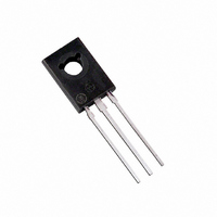
... AND 400 VOLTS 40 WATTS TO−225 CASE 77 STYLE MARKING DIAGRAM 1 BASE YWW 2 COLLECTOR JE 13003G 3 EMITTER Y = Year WW = Work Week JE13003 = Device Code G = Pb−Free Package ORDERING INFORMATION Device Package Shipping MJE13003 TO−225 500 Units/Box TO−225 500 Units/Box MJE13003G (Pb−Free) Publication Order Number: MJE13003/D ...

Page 2

... Fall Time Î Î Î Î Î Î Î Î 2. Pulse Test 300 ms, Duty Cycle v 2%. Î Î Î Î Î Î Î Î Î Î Î Î Î MJE13003 (T = 25_C unless otherwise noted) C Î Î Î Î Î ...

Page 3

... Figure 3. Base−Emitter Voltage 250 150° 125°C 10 100° 75°C 50° 25°C REVERSE FORWARD −1 10 −0.4 −0 BASE−EMITTER VOLTAGE (VOLTS) BE Figure 5. Collector Cutoff Region MJE13003 2 1 0.8 0.4 0 0.5 0 0.002 0.005 Figure 2. Collector Saturation Region 0.2 0.15 0.1 ...

Page 4

... Adjusted for Desired Adjusted for Desired Coil Data: Ferroxcube Core #6656 Full Bobbin (~200 Turns) #20 OUTPUT WAVEFORMS I t CLAMPED C(pk clamp TIME t 2 MJE13003 + MJE210 L MR826* 1N4933 V I clamp *SELECTED FOR ≥ 5 T.U.T. MJE200 47 100 1/2 W − V BE(off) GAP for 30 mH ...

Page 5

... Voltage Rise Time, 10−90 Current Fall Time, 90−10 Current Tail, 10− Crossover Time clamp MJE13003 Table 2. Typical Inductive Switching Performance V clamp Î Î Î Î Î Î Î Î Î Î Î Î 90 AMP t t Î Î Î Î Î Î ...

Page 6

... Figure 8. Turn−On Time 1 0 0.5 0.5 0.3 0.2 0.2 0.1 0.1 0.05 0.07 0.02 0.05 0.03 0.01 0.02 SINGLE PULSE 0.01 0.01 0.02 0.03 0.05 0.1 0.2 MJE13003 0.7 0.5 0.3 0.2 0.1 0.5 0 0.02 0.03 0. r(t) R qJC(t) qJC R = 3.12°C/W MAX ...

Page 7

... This can be accomplished by several means such as active clamping, RC MJE13003 snubbing, load line shaping, etc. The safe level for these devices is specified as Reverse Bias Safe Operating Area and represents the voltage− ...

Page 8

... S 0.025 0.035 0.64 0.88 U 0.145 0.155 3.69 3.93 V 0.040 −−− 1.02 −−− STYLE 3: PIN 1. BASE 2. COLLECTOR 3. EMITTER ON Semiconductor Website: http://onsemi.com Order Literature: http://www.onsemi.com/litorder For additional information, please contact your local Sales Representative. MJE13003/D ...

Related keywords