2N6045 ON Semiconductor, 2N6045 Datasheet
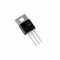
TRANS DARL NPN 8A 100V TO220AB

2N6045

Manufacturer Part Number
2N6045
Description
TRANS DARL NPN 8A 100V TO220AB
Manufacturer
ON Semiconductor
Datasheet

Specifications of 2N6045

Transistor Type
NPN - Darlington
Current - Collector (ic) (max)
8A
Voltage - Collector Emitter Breakdown (max)
100V
Vce Saturation (max) @ Ib, Ic
2V @ 12mA, 3A
Current - Collector Cutoff (max)
20µA
Dc Current Gain (hfe) (min) @ Ic, Vce
1000 @ 3A, 4V
Power - Max
75W
Mounting Type
Through Hole
Package / Case
TO-220-3 (Straight Leads)
Polarity
NPN
Number Of Elements
1
Collector-emitter Voltage
100V
Collector-base Voltage
100V
Emitter-base Voltage
5V
Base-emitter Saturation Voltage (max)
4.5@80mA@8AV
Collector-emitter Saturation Voltage
2@12mA@4A/4@80mA@8AV
Collector Current (dc) (max)
8A
Dc Current Gain
100@8A@4V/1000@3A@4V
Operating Temp Range
-65C to 150C
Operating Temperature Classification
Military
Mounting
Through Hole
Pin Count
3 +Tab
Package Type
TO-220
Lead Free Status / RoHS Status
Contains lead / RoHS non-compliant
Frequency - Transition
-
Lead Free Status / Rohs Status
Not Compliant
Other names
2N6045OS

Available stocks

Company
Part Number
Manufacturer
Quantity
Price
Part Number:
2N6045
Manufacturer:
ON
Quantity:
10 000
Part Number:
2N6045G
Manufacturer:
ON
Quantity:
3 650
Part Number:
2N6045G
Manufacturer:
NXP
Quantity:
10 000
Î Î Î Î Î Î Î Î Î Î Î Î Î Î Î Î Î Î Î
Î Î Î Î Î Î Î Î Î Î Î Î
PNP - 2N6040, 2N6042,
NPN - 2N6043, 2N6045
Plastic Medium-Power
Complementary Silicon
Transistors
designed for general-purpose amplifier and low-speed switching
applications.
Features
Stresses exceeding Maximum Ratings may damage the device. Maximum
Ratings are stress ratings only. Functional operation above the Recommended
Operating Conditions is not implied. Extended exposure to stresses above the
Recommended Operating Conditions may affect device reliability.
1. Indicates JEDEC Registered Data.
*For additional information on our Pb-Free strategy and soldering details, please
© Semiconductor Components Industries, LLC, 2007
November, 2007 - Rev. 8
MAXIMUM RATINGS
Collector-Emitter Voltage
Collector-Base Voltage
Emitter-Base Voltage
Collector Current
Base Current
Total Power Dissipation @ T
Derate above 25°C
Operating and Storage Junction
Temperature Range
download the ON Semiconductor Soldering and Mounting Techniques
Reference Manual, SOLDERRM/D.
Plastic medium-power complementary silicon transistors are
High DC Current Gain - h
Collector-Emitter Sustaining Voltage - @ 100 mAdc -
Low Collector-Emitter Saturation Voltage -
Monolithic Construction with Built-In Base-Emitter Shunt Resistors
Epoxy Meets UL 94 V-0 @ 0.125 in
ESD Ratings:
Pb-Free Packages are Available*
V
= 100 Vdc (Min) - 2N6042, 2N6045
V
= 2.0 Vdc (Max) @ I
Machine Model, C > 400 V
CEO(sus)
CE(sat)
Rating
2N6043 and 2N6045 are Preferred Devices
= 2.0 Vdc (Max) @ I
Human Body Model, 3B > 8000 V
= 60 Vdc (Min) - 2N6040, 2N6043
(Note 1)
C
Continuous
= 25°C
FE
2N6040
2N6043
2N6042
2N6045
2N6040
2N6043
2N6042
2N6045
= 2500 (Typ) @ I
C
Peak
= 3.0 Adc - 2N6042, 2N6045
Î Î Î
Î Î Î
Î Î Î
Î Î Î
Î Î Î
Î Î Î
Î Î Î
Î Î Î
Î Î Î
Î Î Î
Î Î Î
Î Î Î
Î Î Î
Î Î Î
Î Î Î
Î Î Î
Î Î Î
Î Î Î
Î Î Î
Î Î Î
Î Î Î
Symbol
T
C
V
J
V
V
P
CEO
, T
= 4.0 Adc - 2N6043,44
I
I
CB
EB
C
B
D
stg
Î Î Î Î
Î Î Î Î
Î Î Î Î
Î Î Î Î
Î Î Î Î
Î Î Î Î
Î Î Î Î
Î Î Î Î
Î Î Î Î
Î Î Î Î
Î Î Î Î
Î Î Î Î
Î Î Î Î
Î Î Î Î
Î Î Î Î
Î Î Î Î
Î Î Î Î
Î Î Î Î
Î Î Î Î
Î Î Î Î
Î Î Î Î
C
= 4.0 Adc
Value
–65 to
+150
0.60
100
100
120
5.0
8.0
60
60
16
75
Î Î Î
Î Î Î
Î Î Î
Î Î Î
Î Î Î
Î Î Î
Î Î Î
Î Î Î
Î Î Î
Î Î Î
Î Î Î
Î Î Î
Î Î Î
Î Î Î
Î Î Î
Î Î Î
Î Î Î
Î Î Î
Î Î Î
Î Î Î
Î Î Î
1
mAdc
W/°C
Unit
Vdc
Vdc
Vdc
Adc
°C
W
See detailed ordering and shipping information in the package
dimensions section on page 5 of this data sheet.
Preferred devices are recommended choices for future use
and best overall value.
COMPLEMENTARY SILICON
DARLINGTON, 8 AMPERES
60 - 100 VOLTS, 75 WATTS
POWER TRANSISTORS
ORDERING INFORMATION
2N604x = Device Code
A
Y
WW
G
MARKING DIAGRAM
http://onsemi.com
= Assembly Location
= Year
= Work Week
= Pb-Free Package
2N604xG
x = 0, 2, 3, or 5
AYWW
CASE 221A-09
Publication Order Number:
TO-220AB
STYLE 1
2N6040/D

Related parts for 2N6045

2N6045 Summary of contents

Page 1

... High DC Current Gain - h = 2500 (Typ • Collector-Emitter Sustaining Voltage - @ 100 mAdc - Vdc (Min) - 2N6040, 2N6043 CEO(sus) = 100 Vdc (Min) - 2N6042, 2N6045 • Low Collector-Emitter Saturation Voltage - V = 2.0 Vdc (Max CE(sat) = 2.0 Vdc (Max • Monolithic Construction with Built-In Base-Emitter Shunt Resistors • ...

Page 2

... PNP - 2N6040, 2N6042, NPN - 2N6043, 2N6045 Î Î Î Î Î Î Î Î Î Î Î Î Î Î Î Î Î Î Î Î Î Î Î Î Î Î Î Î Î Î Î Î Î THERMAL CHARACTERISTICS Î ...

Page 3

... PNP - 2N6040, 2N6042, NPN - 2N6043, 2N6045 4.0 80 3.0 60 2 & R VARIED TO OBTAIN DESIRED CURRENT LEVELS MUST BE FAST RECOVERY TYPE, eg: 1 ≈ 100 mA 1N5825 USED ABOVE I B ≈ 100 mA MSD6100 USED BELOW approx + 8 4.0 V approx - for t and and ≤ For NPN test circuit reverse all polarities and D1. ...

Page 4

... PNP - 2N6040, 2N6042, NPN - 2N6043, 2N6045 20 10 5.0 500 ms 1.0 ms 2.0 5 150°C J 1.0 BONDING WIRE LIMITED THERMALLY LIMITED @ T = 25°C 0.5 C (SINGLE PULSE) 0.2 SECOND BREAKDOWN LIMITED CURVES APPLY BELOW RATED V CEO 0.1 2N6040, 2N6043 0.05 0.02 1.0 2.0 3.0 5 ...

Page 5

... PNP - 2N6040, 2N6042, NPN - 2N6043, 2N6045 3.0 2 2 2.2 1.8 1.4 1.0 0.3 0.5 0.7 1.0 2.0 3 BASE CURRENT (mA 25°C J 2.5 2 250 BE(sat 1 250 CE(sat 0.5 0.1 0.2 0.3 0.5 0.7 1 COLLECTOR CURRENT (AMP) C ORDERING INFORMATION ...

Page 6

... PNP - 2N6040, 2N6042, NPN - 2N6043, 2N6045 Semiconductor and are registered trademarks of Semiconductor Components Industries, LLC (SCILLC). SCILLC reserves the right to make changes without further notice to any products herein. SCILLC makes no warranty, representation or guarantee regarding the suitability of its products for any particular purpose, nor does SCILLC assume any liability arising out of the application or use of any product or circuit, and specifically disclaims any and all liability, including without limitation special, consequential or incidental damages. “ ...

Related keywords