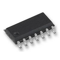
74HCT125D NXP Semiconductors, 74HCT125D Datasheet - Page 2

74HCT125D
Manufacturer Part Number
74HCT125D
Description
Buffer/Line Driver 4-CH Non-Inverting 3-ST CMOS 14-Pin SO Bulk
Manufacturer
NXP Semiconductors
Datasheet
1.74HCT125D.pdf
(6 pages)
Specifications of 74HCT125D
Package
14SO
Logic Family
HCT
Logic Function
Buffer/Line Driver
Number Of Outputs Per Chip
4
Output Type
3-State
Input Signal Type
Single-Ended
Maximum Propagation Delay Time @ Maximum Cl
25@4.5V ns
Polarity
Non-Inverting
Supply Voltage Range
4.5V To 5.5V
Logic Case Style
SOIC
No. Of Pins
14
Operating Temperature Range
-40°C To +125°C
Svhc
No SVHC (18-Jun-2010)
Base Number
74
Ic Generic
RoHS Compliant
Package / Case
SOIC
Logic Device Type
Buffer / Line Driver, Non Inverting
Rohs Compliant
Yes
Lead Free Status / RoHS Status
Available stocks
Company
Part Number
Manufacturer
Quantity
Price
Company:
Part Number:
74HCT125D
Manufacturer:
ST
Quantity:
31 500
Company:
Part Number:
74HCT125D
Manufacturer:
PHILIPS
Quantity:
14
Company:
Part Number:
74HCT125D
Manufacturer:
NXP92
Quantity:
1 800
Part Number:
74HCT125D
Manufacturer:
TI/德州仪器
Quantity:
20 000
Company:
Part Number:
74HCT125D-T
Manufacturer:
Infineon
Quantity:
91
Company:
Part Number:
74HCT125DB,112
Manufacturer:
NXP
Quantity:
10 000
Philips Semiconductors
FEATURES
GENERAL DESCRIPTION
The 74HC/HCT125 are high-speed Si-gate CMOS devices and are pin compatible with low power Schottky TTL (LSTTL).
They are specified in compliance with JEDEC standard no. 7A.
The 74HC/HCT125 are four non-inverting buffer/line drivers with 3-state outputs. The 3-state outputs (nY) are controlled
by the output enable input (nOE). A HIGH at nOE causes the outputs to assume a HIGH impedance OFF-state.
The “125” is identical to the “126” but has active LOW enable inputs.
QUICK REFERENCE DATA
GND = 0 V; T
Notes
1. C
2. For HC the condition is V
ORDERING INFORMATION
See
December 1990
t
C
C
PHL
Output capability: bus driver
I
Quad buffer/line driver; 3-state
I
PD
CC
SYMBOL
f
f
C
V
For HCT the condition is V
i
o
“74HC/HCT/HCU/HCMOS Logic Package Information”
/ t
CC
PD
= input frequency in MHz
L
category: MSI
= output frequency in MHz
(C
PLH
= output load capacitance in pF
P
= supply voltage in V
is used to determine the dynamic power dissipation (P
L
D
= C
V
amb
CC
PD
2
= 25 C; t
propagation delay nA to nY
input capacitance
power dissipation capacitance per buffer
V
f
o
CC
) = sum of outputs
2
f
r
i
= t
+
I
= GND to V
I
f
= GND to V
= 6 ns
PARAMETER
(C
L
V
CC
CC
2
CC
f
o
) where:
1.5 V
2
.
C
notes 1 and 2
D
L
in W):
= 15 pF; V
CONDITIONS
CC
= 5 V
9
3.5
22
HC
TYPICAL
74HC/HCT125
Product specification
12
3.5
24
HCT
UNIT
ns
pF
pF


