MJE210G ON Semiconductor, MJE210G Datasheet - Page 2
MJE210G
Manufacturer Part Number
MJE210G
Description
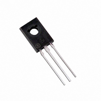
TRANS PWR PNP 5A 25V TO225AA
Manufacturer
ON Semiconductor
Type
Powerr
Specifications of MJE210G
Transistor Type
PNP
Current - Collector (ic) (max)
5A
Voltage - Collector Emitter Breakdown (max)
40V
Vce Saturation (max) @ Ib, Ic
1.8V @ 1A, 5A
Dc Current Gain (hfe) (min) @ Ic, Vce
45 @ 2A, 1V
Power - Max
15W
Frequency - Transition
65MHz
Mounting Type
Through Hole
Package / Case
TO-225-3
Transistor Polarity
PNP
Mounting Style
Through Hole
Collector- Emitter Voltage Vceo Max
40 V
Emitter- Base Voltage Vebo
8 V
Maximum Dc Collector Current
5 A
Power Dissipation
15 W
Maximum Operating Temperature
+ 150 C
Continuous Collector Current
5 A
Dc Collector/base Gain Hfe Min
70
Maximum Operating Frequency
65 MHz
Minimum Operating Temperature
- 65 C
Current, Collector
5 A
Current, Gain
10
Frequency
65 MHz
Package Type
TO-225
Polarity
PNP
Primary Type
Si
Resistance, Thermal, Junction To Case
8.34 °C/W
Voltage, Breakdown, Collector To Emitter
40 V
Voltage, Collector To Base
25 V
Voltage, Collector To Emitter
40 V
Voltage, Collector To Emitter, Saturation
1.8 V
Voltage, Emitter To Base
8 V
Number Of Elements
1
Collector-emitter Voltage
25V
Collector-base Voltage
40V
Emitter-base Voltage
8V
Collector Current (dc) (max)
5A
Dc Current Gain (min)
70
Frequency (max)
65MHz
Operating Temp Range
-65C to 150C
Operating Temperature Classification
Military
Mounting
Through Hole
Pin Count
3 +Tab
Lead Free Status / RoHS Status
Lead free / RoHS Compliant
Current - Collector Cutoff (max)
-
Lead Free Status / Rohs Status
Lead free / RoHS Compliant
Other names
MJE210GOS
Available stocks
Company
Part Number
Manufacturer
Quantity
Price

Part Number:
MJE210G
Manufacturer:
ON/安森美
Quantity:
20 000


Î Î Î Î Î Î Î Î Î Î Î Î Î Î Î Î Î Î Î Î Î Î Î Î Î Î Î Î Î Î Î Î Î
Î Î Î Î Î Î Î Î Î Î Î Î Î Î Î Î Î Î Î Î Î Î Î Î Î Î Î Î Î Î Î Î Î
Î Î Î Î Î Î Î Î Î Î Î Î Î Î Î Î Î Î Î Î Î
Î Î Î Î Î Î Î Î Î Î Î Î Î Î Î Î Î Î Î Î Î
Î Î Î Î Î Î Î Î Î Î Î Î Î Î Î Î Î Î Î Î Î Î Î Î Î Î Î Î Î Î Î Î Î
Î Î Î Î Î Î Î Î Î Î Î Î Î Î Î Î Î Î Î Î Î Î Î Î Î Î Î Î Î Î Î Î Î
Î Î Î Î Î Î Î Î Î Î Î Î Î Î Î Î Î Î Î Î Î
Î Î Î Î Î Î Î Î Î Î Î Î Î Î Î Î Î Î Î Î Î
Î Î Î Î Î Î Î Î Î Î Î Î Î Î Î Î Î Î Î Î Î
Î Î Î Î Î Î Î Î Î Î Î Î Î Î Î Î Î Î Î Î Î
Î Î Î Î Î Î Î Î Î Î Î Î Î Î Î Î Î Î Î Î Î
Î Î Î Î Î Î Î Î Î Î Î Î Î Î Î Î Î Î Î Î Î
Î Î Î Î Î Î Î Î Î Î Î Î Î Î Î Î Î Î Î Î Î
Î Î Î Î Î Î Î Î Î Î Î Î Î Î Î Î Î Î Î Î Î
Î Î Î Î Î Î Î Î Î Î Î Î Î Î Î Î Î Î Î Î Î
Î Î Î Î Î Î Î Î Î Î Î Î Î Î Î Î Î Î Î Î Î Î Î Î Î Î Î Î Î Î Î Î Î
Î Î Î Î Î Î Î Î Î Î Î Î Î Î Î Î Î Î Î Î Î Î Î Î Î Î Î Î Î Î Î Î Î
Î Î Î Î Î Î Î Î Î Î Î Î Î Î Î Î Î Î Î Î Î
Î Î Î Î Î Î Î Î Î Î Î Î Î Î Î Î Î Î Î Î Î
Î Î Î Î Î Î Î Î Î Î Î Î Î Î Î Î Î Î Î Î Î
Î Î Î Î Î Î Î Î Î Î Î Î Î Î Î Î Î Î Î Î Î
Î Î Î Î Î Î Î Î Î Î Î Î Î Î Î Î Î Î Î Î Î
Î Î Î Î Î Î Î Î Î Î Î Î Î Î Î Î Î Î Î Î Î
Î Î Î Î Î Î Î Î Î Î Î Î Î Î Î Î Î Î Î Î Î
Î Î Î Î Î Î Î Î Î Î Î Î Î Î Î Î Î Î Î Î Î
Î Î Î Î Î Î Î Î Î Î Î Î Î Î Î Î Î Î Î Î Î
Î Î Î Î Î Î Î Î Î Î Î Î Î Î Î Î Î Î Î Î Î
Î Î Î Î Î Î Î Î Î Î Î Î Î Î Î Î Î Î Î Î Î
Î Î Î Î Î Î Î Î Î Î Î Î Î Î Î Î Î Î Î Î Î
Î Î Î Î Î Î Î Î Î Î Î Î Î Î Î Î Î Î Î Î Î
Î Î Î Î Î Î Î Î Î Î Î Î Î Î Î Î Î Î Î Î Î
Î Î Î Î Î Î Î Î Î Î Î Î Î Î Î Î Î Î Î Î Î Î Î Î Î Î Î Î Î Î Î Î Î
Î Î Î Î Î Î Î Î Î Î Î Î Î Î Î Î Î Î Î Î Î Î Î Î Î Î Î Î Î Î Î Î Î
Î Î Î Î Î Î Î Î Î Î Î Î Î Î Î Î Î Î Î Î Î
Î Î Î Î Î Î Î Î Î Î Î Î Î Î Î Î Î Î Î Î Î
Î Î Î Î Î Î Î Î Î Î Î Î Î Î Î Î Î Î Î Î Î
Î Î Î Î Î Î Î Î Î Î Î Î Î Î Î Î Î Î Î Î Î
Î Î Î Î Î Î Î Î Î Î Î Î Î Î Î Î Î Î Î Î Î
Î Î Î Î Î Î Î Î Î Î Î Î Î Î Î Î Î Î Î Î Î
1. Pulse Test: Pulse Width = 300 ms, Duty Cycle [ 2.0%.
2. f
ELECTRICAL CHARACTERISTICS
OFF CHARACTERISTICS
ON CHARACTERISTICS
DYNAMIC CHARACTERISTICS
Collector-Emitter Sustaining Voltage (Note 1)
Collector Cutoff Current
Emitter Cutoff Current
DC Current Gain (Note 1)
Collector-Emitter Saturation Voltage (Note 1)
Base-Emitter Saturation Voltage (Note 1)
Base-Emitter On Voltage (Note 1)
Current-Gain - Bandwidth Product (Note 2)
Output Capacitance
T
(I
(V
(V
(V
(I
(I
(I
(I
(I
(I
(I
(I
(I
(V
C
C
C
C
C
C
C
C
C
C
= ⎪h
CB
CB
BE
CB
= 10 mAdc, I
= 500 mAdc, V
= 2.0 Adc, V
= 5.0 Adc, V
= 500 mAdc, I
= 2.0 Adc, I
= 5.0 Adc, I
= 5.0 Adc, I
= 2.0 Adc, V
= 100 mAdc, V
= 8.0 Vdc, I
= 40 Vdc, I
= 40 Vdc, I
= 10 Vdc, I
fe
⎪• f
test
.
B
B
B
CE
CE
CE
B
E
E
E
= 200 mAdc)
= 1.0 Adc)
= 1.0 Adc)
C
B
= 0)
= 0)
= 0, T
CE
CE
= 0, f = 0.1 MHz)
= 0)
= 1.0 Vdc)
= 2.0 Vdc)
= 1.0 Vdc)
= 50 mAdc)
= 1.0 Vdc)
= 10 Vdc, f
J
= 125_C)
Characteristic
test
8.0
4.0
16
12
0
20
= 10 MHz)
(T
MJE200 - NPN,
C
= 25_C unless otherwise noted)
40
Figure 1. Power Derating
60
http://onsemi.com
T, TEMPERATURE (°C)
80
2
100
MJE210 - PNP
MJE200
MJE210
120
Î Î Î Î Î
Î Î Î Î Î
Î Î Î Î Î
Î Î Î Î Î
Î Î Î Î Î
Î Î Î Î Î
Î Î Î Î Î
Î Î Î Î Î
Î Î Î Î Î
Î Î Î Î Î
Î Î Î Î Î
Î Î Î Î Î
Î Î Î Î Î
Î Î Î Î Î
Î Î Î Î Î
Î Î Î Î Î
Î Î Î Î Î
Î Î Î Î Î
Î Î Î Î Î
Î Î Î Î Î
Î Î Î Î Î
Î Î Î Î Î
Î Î Î Î Î
Î Î Î Î Î
Î Î Î Î Î
Î Î Î Î Î
Î Î Î Î Î
Î Î Î Î Î
Î Î Î Î Î
Î Î Î Î Î
Î Î Î Î Î
140
V
Symbol
V
V
V
CEO(sus)
I
CE(sat)
BE(sat)
I
BE(on)
h
C
CBO
EBO
f
FE
T
ob
160
1.6
1.2
0.8
0.4
0
Î Î Î Î
Î Î Î Î
Î Î Î Î
Î Î Î Î
Î Î Î Î
Î Î Î Î
Î Î Î Î
Î Î Î Î
Î Î Î Î
Î Î Î Î
Î Î Î Î
Î Î Î Î
Î Î Î Î
Î Î Î Î
Î Î Î Î
Î Î Î Î
Î Î Î Î
Î Î Î Î
Î Î Î Î
Î Î Î Î
Î Î Î Î
Î Î Î Î
Î Î Î Î
Î Î Î Î
Î Î Î Î
Î Î Î Î
Î Î Î Î
Î Î Î Î
Î Î Î Î
Î Î Î Î
Î Î Î Î
Min
25
70
45
10
65
-
-
-
-
-
-
-
-
-
-
Î Î Î
Î Î Î
Î Î Î
Î Î Î
Î Î Î
Î Î Î
Î Î Î
Î Î Î
Î Î Î
Î Î Î
Î Î Î
Î Î Î
Î Î Î
Î Î Î
Î Î Î
Î Î Î
Î Î Î
Î Î Î
Î Î Î
Î Î Î
Î Î Î
Î Î Î
Î Î Î
Î Î Î
Î Î Î
Î Î Î
Î Î Î
Î Î Î
Î Î Î
Î Î Î
Î Î Î
Max
0.75
100
100
100
180
120
0.3
1.8
2.5
1.6
80
-
-
-
-
Î Î Î Î
Î Î Î Î
Î Î Î Î
Î Î Î Î
Î Î Î Î
Î Î Î Î
Î Î Î Î
Î Î Î Î
Î Î Î Î
Î Î Î Î
Î Î Î Î
Î Î Î Î
Î Î Î Î
Î Î Î Î
Î Î Î Î
Î Î Î Î
Î Î Î Î
Î Î Î Î
Î Î Î Î
Î Î Î Î
Î Î Î Î
Î Î Î Î
Î Î Î Î
Î Î Î Î
Î Î Î Î
Î Î Î Î
Î Î Î Î
Î Î Î Î
Î Î Î Î
Î Î Î Î
Î Î Î Î
nAdc
mAdc
nAdc
MHz
Unit
Vdc
Vdc
Vdc
Vdc
pF
-
Related parts for MJE210G
Image
Part Number
Description
Manufacturer
Datasheet
Request
R

Part Number:
Description:
ON Semiconductor [VOLTAGE REGULATOR]
Manufacturer:
ON Semiconductor
Datasheet:
Part Number:
Description:
357-036-542-201 CARDEDGE 36POS DL .156 BLK LOPRO
Manufacturer:
ON Semiconductor
Datasheet:
Part Number:
Description:
357-036-542-201 CARDEDGE 36POS DL .156 BLK LOPRO
Manufacturer:
ON Semiconductor
Datasheet:
Part Number:
Description:
357-036-542-201 CARDEDGE 36POS DL .156 BLK LOPRO
Manufacturer:
ON Semiconductor
Datasheet:
Part Number:
Description:
357-036-542-201 CARDEDGE 36POS DL .156 BLK LOPRO
Manufacturer:
ON Semiconductor
Datasheet:
Part Number:
Description:
357-036-542-201 CARDEDGE 36POS DL .156 BLK LOPRO
Manufacturer:
ON Semiconductor
Datasheet:
Part Number:
Description:
357-036-542-201 CARDEDGE 36POS DL .156 BLK LOPRO
Manufacturer:
ON Semiconductor
Datasheet:
Part Number:
Description:
357-036-542-201 CARDEDGE 36POS DL .156 BLK LOPRO
Manufacturer:
ON Semiconductor
Datasheet:
Part Number:
Description:
357-036-542-201 CARDEDGE 36POS DL .156 BLK LOPRO
Manufacturer:
ON Semiconductor
Datasheet:
Part Number:
Description:
357-036-542-201 CARDEDGE 36POS DL .156 BLK LOPRO
Manufacturer:
ON Semiconductor
Datasheet:
Part Number:
Description:
357-036-542-201 CARDEDGE 36POS DL .156 BLK LOPRO
Manufacturer:
ON Semiconductor
Datasheet:
Part Number:
Description:
Manufacturer:
ON Semiconductor
Datasheet:
Part Number:
Description:
Manufacturer:
ON Semiconductor
Datasheet:
Part Number:
Description:
Manufacturer:
ON Semiconductor
Datasheet: