Î Î Î Î Î Î Î Î Î Î Î Î
Î Î Î Î Î Î Î Î Î Î Î Î
Î Î Î Î Î Î Î Î Î Î Î Î
Î Î Î Î Î Î Î Î Î Î Î Î
Î Î Î Î Î Î Î Î Î Î Î Î
Î Î Î Î Î Î Î Î Î Î Î Î
Î Î Î Î Î Î Î Î Î Î Î Î
Î Î Î Î Î Î Î Î Î Î Î Î
Î Î Î Î Î Î Î Î Î Î Î Î
Î Î Î Î Î Î Î Î Î Î Î Î
Î Î Î Î Î Î Î Î Î Î Î Î
Î Î Î Î Î Î Î Î Î Î Î Î
Î Î Î Î Î Î Î Î Î Î Î Î
Î Î Î Î Î Î Î Î Î Î Î Î
Î Î Î Î Î Î Î Î Î Î Î Î
Î Î Î Î Î Î Î Î Î Î Î Î
Î Î Î Î Î Î Î Î Î Î Î Î
Î Î Î Î Î Î Î Î Î Î Î Î
Î Î Î Î Î Î Î Î Î Î Î Î Î Î Î Î Î Î Î
Î Î Î Î Î Î Î Î Î Î Î Î Î Î Î Î Î Î Î
Î Î Î Î Î Î Î Î Î Î Î Î
Î Î Î Î Î Î Î Î Î Î Î Î
Î Î Î Î Î Î Î Î Î Î Î Î
Î Î Î Î Î Î Î Î Î Î Î Î
Î Î Î Î Î Î Î Î Î Î Î Î
Î Î Î Î Î Î Î Î Î Î Î Î
Î Î Î Î Î Î Î Î Î Î Î Î
Î Î Î Î Î Î Î Î Î Î Î Î
Î Î Î Î Î Î Î Î Î Î Î Î
Î Î Î Î Î Î Î Î Î Î Î Î
Î Î Î Î Î Î Î Î Î Î Î Î
Î Î Î Î Î Î Î Î Î Î Î Î
MJB41C (NPN),
MJB42C (PNP)
Complementary Silicon
Plastic Power Transistors
D
Features
•
•
•
Maximum ratings are those values beyond which device damage can occur.
Maximum ratings applied to the device are individual stress limit values (not
normal operating conditions) and are not valid simultaneously. If these limits are
exceeded, device functional operation is not implied, damage may occur and
reliability may be affected.
1. I
2. When surface mounted to an FR−4 board using the minimum recommended
MAXIMUM RATINGS
THERMAL CHARACTERISTICS
© Semiconductor Components Industries, LLC, 2005
December, 2005 − Rev. 1
Collector−Emitter Voltage
Collector−Base Voltage
Emitter−Base Voltage
Collector Current
Base Current
Total Power Dissipation
Total Power Dissipation
Unclamped Inductive Load Energy (Note 1)
Operating and Storage Junction
Temperature Range
Thermal Resistance, Junction−to−Case
Thermal Resistance,
Thermal Resistance,
Maximum Lead Temperature for Soldering
Purposes, 1/8″ from Case for 10 Seconds
2
(No Suffix)
Lead Formed for Surface Mount Applications in Plastic Sleeves
Electrically the Same as TIP41 and T1P42 Series
Pb−Free Packages are Available
pad size.
C
PAK for Surface Mount
= 2.5 A, L = 20 mH, P.R.F. = 10 Hz, V
@ T
Derate above 25_C
@ T
Derate above 25_C
Junction−to−Ambient
Junction−to−Ambient (Note 2)
Characteristic
A
C
= 25_C
= 25_C
Rating
− Continuous
− Peak
Preferred Devices
CC
Î Î Î
Î Î Î
Î Î Î
Î Î Î
Î Î Î
Î Î Î
Î Î Î
Î Î Î
Î Î Î
Î Î Î
Î Î Î
Î Î Î
Î Î Î
Î Î Î
Î Î Î
Î Î Î
Î Î Î
Î Î Î
Î Î Î
Î Î Î
Î Î Î
Î Î Î
Î Î Î
Î Î Î
Î Î Î
Î Î Î
Î Î Î
Î Î Î
Î Î Î
Î Î Î
Symbol
Symbol
T
V
= 10 V, R
R
R
R
J
V
V
P
P
, T
CEO
T
I
I
qJC
E
qJA
qJA
CB
EB
C
B
D
D
L
stg
Î Î Î Î
Î Î Î Î
Î Î Î Î
Î Î Î Î
Î Î Î Î
Î Î Î Î
Î Î Î Î
Î Î Î Î
Î Î Î Î
Î Î Î Î
Î Î Î Î
Î Î Î Î
Î Î Î Î
Î Î Î Î
Î Î Î Î
Î Î Î Î
Î Î Î Î
Î Î Î Î
Î Î Î Î
Î Î Î Î
Î Î Î Î
Î Î Î Î
Î Î Î Î
Î Î Î Î
Î Î Î Î
Î Î Î Î
Î Î Î Î
Î Î Î Î
Î Î Î Î
Î Î Î Î
−65 to +150
BE
Value
0.016
= 100 W
0.52
62.5
Max
1.92
62.5
100
100
260
5.0
6.0
2.0
2.0
10
65
50
Î Î Î
Î Î Î
Î Î Î
Î Î Î
Î Î Î
Î Î Î
Î Î Î
Î Î Î
Î Î Î
Î Î Î
Î Î Î
Î Î Î
Î Î Î
Î Î Î
Î Î Î
Î Î Î
Î Î Î
Î Î Î
Î Î Î
Î Î Î
Î Î Î
Î Î Î
Î Î Î
Î Î Î
Î Î Î
Î Î Î
Î Î Î
Î Î Î
Î Î Î
Î Î Î
1
W/_C
W/_C
_C/W
_C/W
_C/W
Unit
Unit
Vdc
Vdc
Vdc
Adc
Adc
mJ
_C
_C
W
W
†For information on tape and reel specifications,
Preferred devices are recommended choices for future use
and best overall value.
including part orientation and tape sizes, please
refer to our Tape and Reel Packaging Specifications
Brochure, BRD8011/D.
MJB41C
MJB41CG
MJB41CT4
MJB41CT4G
MJB42C
MJB42CG
MJB42CT4
MJB42CT4G
COMPLEMENTARY SILICON
Device
POWER TRANSISTORS
100 VOLTS, 65 WATTS
J4xC
A
Y
WW
G
ORDERING INFORMATION
http://onsemi.com
6 AMPERES,
= Specific Device Code
= Assembly Location
= Year
= Work Week
= Pb−Free Package
x = 1 or 2
(Pb−Free)
(Pb−Free)
(Pb−Free)
(Pb−Free)
Package
D
D
D
D
D
D
D
D
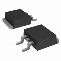
CASE 418B
STYLE 1
2
2
2
2
2
2
2
2
D
PAK
PAK
PAK
PAK
PAK
PAK
PAK
PAK
Publication Order Number:
2
PAK
800/Tape & Reel
800/Tape & Reel
800/Tape & Reel
800/Tape & Reel
50 Units/Rail
50 Units/Rail
50 Units/Rail
50 Units/Rail
MARKING
DIAGRAM
Shipping
J4xCG
AYWW
MJB41C/D
†