BC817-40LT3G ON Semiconductor, BC817-40LT3G Datasheet
BC817-40LT3G
Specifications of BC817-40LT3G
Available stocks


Related parts for BC817-40LT3G


BC817-40LT3G Summary of contents
Page 1
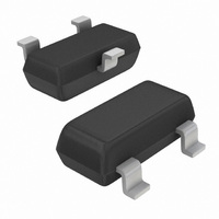
... COLLECTOR 3 1 BASE 2 EMITTER SOT−23 CASE 318 STYLE 6 MARKING DIAGRAM Device Code Date Code* = Pb−Free Package G (Note: Microdot may be in either location) *Date Code orientation and/or overbar may vary depending upon manufacturing location. ORDERING INFORMATION Publication Order Number: BC817−16LT1/D ...
Page 2
... Tape and Reel Packaging Specifications Brochure, BRD8011/ 25°C unless otherwise noted) A Symbol V (BR)CEO V (BR)CES V (BR)EBO BC817−16 BC817−25 BC817− Specific Marking Package SOT−23 (Pb−Free) 6A SOT−23 (Pb−Free) SOT− ...
Page 3
... TYPICAL CHARACTERISTICS − BC817−16LT1 300 150°C 200 25°C −55°C 100 0 0.001 0. COLLECTOR CURRENT (A) C Figure 1. DC Current Gain vs. Collector Current 1.1 1 0.9 0.8 0.7 0.6 0.5 0.4 0.3 0.2 0.0001 0.001 0. COLLECTOR CURRENT (A) C Figure 3. Base Emitter Saturation Voltage vs. ...
Page 4
... TYPICAL CHARACTERISTICS − BC817−16LT1 1 25°C J 0.8 0 100 mA 300 mA C 0.4 0.2 0 0.01 0 BASE CURRENT (mA) B Figure 5. Saturation Region 100 500 100 1 Figure 6. Temperature Coefficients REVERSE VOLTAGE (VOLTS) R Figure 7. Capacitances http://onsemi.com 4 for V CE(sat) q for 100 I , COLLECTOR CURRENT (mA) ...
Page 5
... TYPICAL CHARACTERISTICS − BC817−25LT1 500 150°C 400 300 25°C 200 −55°C 100 0 0.001 0. COLLECTOR CURRENT (A) C Figure 8. DC Current Gain vs. Collector Current 1.1 1 0.9 0.8 0.7 0.6 0.5 0.4 0.3 0.2 0.0001 0.001 0. COLLECTOR CURRENT (A) C Figure 10. Base Emitter Saturation Voltage vs. ...
Page 6
... TYPICAL CHARACTERISTICS − BC817−25LT1 1 25°C J 0.8 0 100 mA 300 mA C 0.4 0.2 0 0.01 0 BASE CURRENT (mA) B Figure 13. Saturation Region 100 500 100 1 Figure 14. Temperature Coefficients REVERSE VOLTAGE (VOLTS) R Figure 15. Capacitances http://onsemi.com 6 for V CE(sat) q for 100 I , COLLECTOR CURRENT (mA) ...
Page 7
... TYPICAL CHARACTERISTICS − BC817−40LT1 700 150°C 600 500 25°C 400 300 −55°C 200 100 0 0.001 0. COLLECTOR CURRENT (A) C Figure 16. DC Current Gain vs. Collector Current 1.1 1 0.9 0.8 0.7 0.6 0.5 0.4 0.3 0.2 0.0001 0.001 0. COLLECTOR CURRENT (A) C Figure 18. Base Emitter Saturation Voltage vs. ...
Page 8
... TYPICAL CHARACTERISTICS − BC817−40LT1 1 25°C J 0.8 0 100 mA 300 mA C 0.4 0.2 0 0.01 0 BASE CURRENT (mA) B Figure 21. Saturation Region 100 500 100 1 Figure 22. Temperature Coefficients REVERSE VOLTAGE (VOLTS) R Figure 23. Capacitances http://onsemi.com 8 for V CE(sat) q for 100 I , COLLECTOR CURRENT (mA) ...
Page 9
... TYPICAL CHARACTERISTICS − BC817−16LT1, BC817−25LT1, BC817−40LT1 1 Thermal Limit 0.1 0.01 Single Pulse Test @ T A 0.001 0.01 0.1 Figure 24. Safe Operating Area http://onsemi.com 1 ms 100 25° 100 V (Vdc ...
Page 10
... E STYLE 6: PIN 1. BASE 2. EMITTER 3. COLLECTOR 2.0 mm inches ON Semiconductor Website: www.onsemi.com Order Literature: http://www.onsemi.com/orderlit For additional information, please contact your local Sales Representative BC817−16LT1/D MAX 0.044 0.004 0.020 0.007 0.120 0.055 0.081 0.012 0.029 0.104 ...