TC1264-3.0VAB Microchip Technology, TC1264-3.0VAB Datasheet - Page 2
TC1264-3.0VAB
Manufacturer Part Number
TC1264-3.0VAB
Description
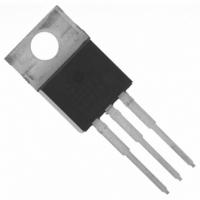
LDO Regulator Pos 3V 0.8A 3-Pin (3+Tab) TO-220
Manufacturer
Microchip Technology
Type
Linearr
Datasheets
1.TC1264-1.8VEBTR.pdf
(20 pages)
2.TC1264-3.0VAB.pdf
(18 pages)
3.TC1264-3.3VAB.pdf
(12 pages)
Specifications of TC1264-3.0VAB
Package
3TO-220
Function
LDO
Number Of Outputs
1
Input Voltage Range
6 to 2.7 V
Output Voltage
3 V
Maximum Output Current
0.8(Min) A
Output Type
Fixed
Accuracy
±0.5 %
Typical Dropout Voltage @ Current
0.02@100uA|0.05@100mA|0.15@300mA|0.26@500mA|0.45@800mA V
Operating Temperature
-40 to 125 °C
Polarity
Positive
Regulator Topology
Positive Fixed
Voltage - Output
3V
Voltage - Input
Up to 6V
Voltage - Dropout (typical)
1.2V @ 800mA
Number Of Regulators
1
Current - Output
800mA (Min)
Mounting Type
Through Hole
Package / Case
TO-220-3
Input Voltage Max
6 V
Dropout Voltage (max)
1400 mV
Output Current
800 mA
Line Regulation
0.001 %
Load Regulation
0 % / mA
Voltage Regulation Accuracy
0.5 %
Maximum Operating Temperature
+ 125 C
Mounting Style
Through Hole
Minimum Operating Temperature
- 40 C
Lead Free Status / RoHS Status
Lead free / RoHS Compliant
Current - Limit (min)
-
Lead Free Status / Rohs Status
Lead free / RoHS Compliant
Other names
TC12643.0VAB
Available stocks
Company
Part Number
Manufacturer
Quantity
Price
Company:

Part Number:
TC1264-3.0VAB
Manufacturer:
MICROCHIP
Quantity:
12 000


TC1264
1.0
Absolute Maximum Ratings †
Input Voltage .........................................................6.5V
Output Voltage.................. (V
Power Dissipation................Internally Limited
Maximum Voltage on Any Pin ........V
Operating Temperature Range...... -40°C < T
Storage Temperature..........................-65°C to +150°C
DC CHARACTERISTICS
DS21375D-page 2
Electrical Specifications: Unless otherwise indicated, V
T
Input Operating Voltage
Maximum Output Current
Output Voltage
V
Line Regulation
Load Regulation
Dropout Voltage
Supply Current
Power Supply Rejection Ratio
Output Short Circuit Current
Note 1:
A
OUT
= +25°C. Boldface type specifications apply for junction temperatures of -40°C to +125°C.
Temperature Coefficient
2:
3:
4:
5:
6:
7:
8:
ELECTRICAL
CHARACTERISTICS
Parameters
V
The minimum V
This accuracy represents the worst-case over the entire output current and temperature range.
Regulation is measured at a constant junction temperature using low duty cycle pulse testing. Load regulation is tested
over a load range from 0.1 mA to the maximum specified output current. Changes in output voltage due to heating
effects are covered by the thermal regulation specification.
Dropout voltage is defined as the input-to-output differential at which the output voltage drops 2% below its nominal
value measured at a 1.5V differential.
Thermal regulation is defined as the change in output voltage at a time T after a change in power dissipation is applied,
excluding load or line regulation effects. Specifications are for a current pulse equal to I
The maximum allowable power dissipation is a function of ambient temperature, the maximum allowable junction
temperature and the thermal resistance from junction-to-air (i.e., T
dissipation causes the device to initiate thermal shutdown. Please see
more details.
TCV
R
is the regulator output voltage setting.
(Note
(Note
OUT
6)
5)
=
------------------------------------------------------------------------ -
V
IN
OUTMAX
has to justify the conditions: V
SS
– 0.3V) to (V
V
V
V
OUT
V
V
–
I
OUTMAX
OUT
IN
I
PSRR
OUT
OUTSC
V
V
Sym
OUT
IN
V
–V
I
OUT
DD
OUTMIN
IN
/V
/V
+0.3V to -0.3V
OUT
/T
OUT
T
IN
IN
J
10
(Note
< 125°C
+ 0.3V)
–
V
V
V
R
R
R
-0.01
Min
800
– 2.5% V
2.7
—
—
—
—
—
—
—
—
—
—
—
—
6
– 2%
– 7%
IN
8)
= V
IN
V
R
+ 1.5V,
V
R
R
R
0.007
0.002
1000
1200
1200
+ V
Typ
± 0.5% V
± 0.5%
150
260
450
40
20
50
80
64
—
—
—
† Notice: Stresses above those listed under "Maximum
Ratings" may cause permanent damage to the device. This is
a stress rating only and functional operation of the device at
those or any other conditions above those indicated in the
operation listings of this specification is not implied. Exposure
to maximum rating conditions for extended periods may affect
device reliability.
DROPOUT
(Note
A
V
V
, T
1), I
R
R
R
1300
1200
1400
Max
0.35
+ 2.5%
160
480
800
130
and V
6.0
J
30
—
—
—
—
+ 3%
+ 3%
0
,
L
Section 5.0 “Thermal Considerations”
= 100 µA, C
JA
). Exceeding the maximum allowable power
IN
2.7V for I
ppm/°C
%/mA
Units
mA
mV
mA
µA
db
%
V
V
L
2010 Microchip Technology Inc.
= 3.3 µF, SHDN > V
LMAX
Note 2
V
V
I
(Note
Note 4
(V
I
V
V
V
V
V
V
SHDN = V
F 1 kHz
V
L
L
L
R
R
R
R
R
R
R
R
OUT
= 0.1 mA to I
= 0.1 mA to 800 mA
R
= 0.1 mA to I
2.5V
= 1.8V
2.5V, I
2.5V,
2.5V,
2.5V,
2.5V,
= 1.8V, I
at V
+ 1V) V
= 0V
3)
IN
Conditions
IH
= 6V for T = 10 ms.
I
I
I
I
L
L
L
L
L
L
I
, I
L
= 100 µA
= 500 mA
IN
=
= 300 mA
= 500 mA
= 800 mA
= 800 mA
L
OUTMAX
OUTMAX
6V
100
= 0
IH
,
mA
.
for
Related parts for TC1264-3.0VAB
Image
Part Number
Description
Manufacturer
Datasheet
Request
R

Part Number:
Description:
IC CMOS LDO 2.5V 800MA SOT223-3
Manufacturer:
Microchip Technology
Datasheet:
Part Number:
Description:
IC CMOS LDO 800MA 2.5V SOT-223
Manufacturer:
Microchip Technology
Datasheet:
Part Number:
Description:
Voltage Regulator
Manufacturer:
Microchip Technology
Datasheet:

Part Number:
Description:
IC CMOS LDO 3.0V 800MA DDPAK-3
Manufacturer:
Microchip Technology
Datasheet:
Part Number:
Description:
IC CMOS LDO 1.8V 800MA DDPAK-3
Manufacturer:
Microchip Technology
Datasheet:

Part Number:
Description:
IC CMOS LDO 1.8V 800MA TO220-3
Manufacturer:
Microchip Technology
Datasheet:

Part Number:
Description:
IC CMOS LDO 3.3V 800MA TO220-3
Manufacturer:
Microchip Technology
Datasheet:

Part Number:
Description:
IC CMOS LDO 2.5V 800MA TO220-3
Manufacturer:
Microchip Technology
Datasheet:
Part Number:
Description:
IC CMOS LDO 3.0V 800MA SOT223-3
Manufacturer:
Microchip Technology
Datasheet:
Part Number:
Description:
IC CMOS LDO 3.0V 800MA SOT223-3
Manufacturer:
Microchip Technology
Datasheet:
Part Number:
Description:
IC CMOS LDO 2.5V 800MA DDPAK-3
Manufacturer:
Microchip Technology
Datasheet:
Part Number:
Description:
IC CMOS LDO 3.3V 800MA DDPAK-3
Manufacturer:
Microchip Technology
Datasheet:
Part Number:
Description:
IC CMOS LDO 1.8V 800MA SOT223-3
Manufacturer:
Microchip Technology
Datasheet:
Part Number:
Description:
Voltage Regulator
Manufacturer:
Microchip Technology
Datasheet:
Part Number:
Description:
Analog IC
Manufacturer:
Microchip Technology
Datasheet: