MAX9626ETC+ Maxim Integrated Products, MAX9626ETC+ Datasheet - Page 2
MAX9626ETC+
Manufacturer Part Number
MAX9626ETC+
Description
RF Amplifier EVAL KIT MAX9626ETC+
Manufacturer
Maxim Integrated Products
Datasheet
1.MAX9627ETC.pdf
(20 pages)
Specifications of MAX9626ETC+
Bandwidth
1150 MHz
Operating Supply Voltage
2.85 V to 5.25 V
Supply Current
59 mA
Maximum Power Dissipation
1333 mW
Maximum Operating Temperature
+ 125 C
Mounting Style
SMD/SMT
Package / Case
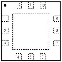
TQFN-12
Minimum Operating Temperature
- 40 C
Lead Free Status / RoHS Status
Lead free / RoHS Compliant


Low-Noise, Low-Distortion,
1.35GHz Fully Differential Amplifiers
ABSOLUTE MAXIMUM RATINGS
Supply Voltage (V
IN+, IN- ...........................................(V
RT+, RT- .........................................(V
RT- to IN- and RT+ to IN+ .................................................... Q2V
VOCM, SHDN, OUT+, OUT- ..........(V
Output Short-Circuit Duration (OUT+ to OUT-) ....................... 1s
Continuous Input Current
ELECTRICAL CHARACTERISTICS
(V
+125°C. Typical values are at +25°C, unless otherwise noted.) (Note 1)
Stresses beyond those listed under “Absolute Maximum Ratings” may cause permanent damage to the device. These are stress ratings only, and functional
operation of the device at these or any other conditions beyond those indicated in the operational sections of the specifications is not implied. Exposure to absolute
maximum rating conditions for extended periods may affect device reliability.
2
DC SPECIFICATIONS
Supply Voltage Range
Supply Current
Power-Supply Rejection Ratio
Differential Voltage Gain
Gain Error
Input Offset Voltage
Common-Mode Input Voltage
Range (Note 2)
CC
(any pin except V
= +3.3V, V
PARAMETER
EE
CC
= 0V, V
EE
to V
, V
CC
EE
IN-
)................................-0.3V to +5.5V
, OUT+, OUT-) .................... Q20mA
= V
IN+
SYMBOL
EE
EE
EE
= 0V, SHDN = V
G
PSRR
V
V
I
- 2.5V) to (V
- 2.5V) to (V
- 0.3V) to (V
DIFF
CC
ICM
CC
Guaranteed by PSRR
SHDN = V
SHDN = GND
V
2.85V P V
-40NC P T
V
2.85V P V
-40NC P T
V
V
Differential input,
V
T
Differential input,
V
T
Guaranteed by CMRR
A
A
VCOM
VCOM
OUT+,
OUT+,
IN-
IN-
CC
CC
CC
= +25NC
= -40°C to +125NC
= V
= V
CC
+ 0.3V)
+ 0.3V)
+ 0.3V)
= V
= V
V
V
IN+
IN+
, V
OUT-
OUT-
A
A
CC
CC
CC
VOCM
CC
CC
P +85NC
P +125NC
= V
= V
P 5.25V,
P 5.25V,
CONDITIONS
/2,
/2,
= -1V to +1V
= -1V to +1V
CC
CC
= V
/2,
/2
Continuous Power Dissipation (T
12-Pin TQFN Multilayer Board (deration 16.7mW/NC
Operating Temperature Range ........................ -40NC to +125NC
Junction Temperature .....................................................+150NC
Storage Temperature Range ............................ -65NC to +150NC
Lead Temperature (soldering, 10s) ................................+300NC
Soldering Temperature (reflow) ......................................+260NC
above +70NC) ..........................................................1333.3mW
CC
B JA ........................................................................60mW/NC
B JC ........................................................................11mW/NC
/2, R
L
= 500I (between OUT+ and OUT-), T
MAX9626
MAX9627
MAX9628
MAX9626
MAX9627
MAX9628
MAX9626
MAX9627
MAX9628
MAX9626
MAX9627
MAX9628
MAX9626
MAX9627
MAX9628
MAX9626
MAX9627
MAX9628
MAX9626
MAX9627
MAX9628
-0.75
MIN
2.85
-1.5
-0.4
66
66
64
60
63
64
-2
-2
-2
A
= +70NC)
TYP
±0.2
±0.2
±0.2
59
25
89
92
92
89
92
92
1
2
4
2
2
2
2
2
2
MAX
+1.5
+1.5
+1.5
5.25
±11
±13
±10
±10
+2
+2
+2
80
50
±8
±8
A
= -40°C to
UNITS
mA
V/V
mV
FA
dB
%
V
V
Related parts for MAX9626ETC+
Image
Part Number
Description
Manufacturer
Datasheet
Request
R

Part Number:
Description:
MAX7528KCWPMaxim Integrated Products [CMOS Dual 8-Bit Buffered Multiplying DACs]
Manufacturer:
Maxim Integrated Products
Datasheet:
Part Number:
Description:
Single +5V, fully integrated, 1.25Gbps laser diode driver.
Manufacturer:
Maxim Integrated Products
Datasheet:
Part Number:
Description:
Single +5V, fully integrated, 155Mbps laser diode driver.
Manufacturer:
Maxim Integrated Products
Datasheet:
Part Number:
Description:
VRD11/VRD10, K8 Rev F 2/3/4-Phase PWM Controllers with Integrated Dual MOSFET Drivers
Manufacturer:
Maxim Integrated Products
Datasheet:
Part Number:
Description:
Highly Integrated Level 2 SMBus Battery Chargers
Manufacturer:
Maxim Integrated Products
Datasheet:
Part Number:
Description:
Current Monitor and Accumulator with Integrated Sense Resistor; ; Temperature Range: -40°C to +85°C
Manufacturer:
Maxim Integrated Products
Part Number:
Description:
TSSOP 14/A�/RS-485 Transceivers with Integrated 100O/120O Termination Resis
Manufacturer:
Maxim Integrated Products
Part Number:
Description:
TSSOP 14/A�/RS-485 Transceivers with Integrated 100O/120O Termination Resis
Manufacturer:
Maxim Integrated Products
Part Number:
Description:
QFN 16/A�/AC-DC and DC-DC Peak-Current-Mode Converters with Integrated Step
Manufacturer:
Maxim Integrated Products
Part Number:
Description:
TDFN/A/65V, 1A, 600KHZ, SYNCHRONOUS STEP-DOWN REGULATOR WITH INTEGRATED SWI
Manufacturer:
Maxim Integrated Products
Part Number:
Description:
Integrated Temperature Controller f
Manufacturer:
Maxim Integrated Products
Part Number:
Description:
SOT23-6/I�/45MHz to 650MHz, Integrated IF VCOs with Differential Output
Manufacturer:
Maxim Integrated Products
Part Number:
Description:
SOT23-6/I�/45MHz to 650MHz, Integrated IF VCOs with Differential Output
Manufacturer:
Maxim Integrated Products
Part Number:
Description:
EVALUATION KIT/2.4GHZ TO 2.5GHZ 802.11G/B RF TRANSCEIVER WITH INTEGRATED PA
Manufacturer:
Maxim Integrated Products
Part Number:
Description:
QFN/E/DUAL PCIE/SATA HIGH SPEED SWITCH WITH INTEGRATED BIAS RESISTOR
Manufacturer:
Maxim Integrated Products
Datasheet: