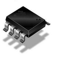
ATA2525XXX-DDW Atmel, ATA2525XXX-DDW Datasheet

ATA2525XXX-DDW
Specifications of ATA2525XXX-DDW
Related parts for ATA2525XXX-DDW
ATA2525XXX-DDW Summary of contents
Page 1
Features • No External Components Except PIN Diode • Supply-voltage Range: 4.5V to 5.5V • High Sensitivity Due to Automatic Sensitivity Adaption (AGC) and Automatic Strong Signal Adaption (ATC) • High Immunity Against Disturbances from Daylight and Lamps • Small ...
Page 2
Figure 1-1. Block Diagram IN Carrier frequency f 0 Modulated IR signal min 10 pulses ATA2525 2 VS CGA and Input filter AGC/ATC Oscillator and digital control GND OUT Micro- Demodulator controller ATA2525 4854G–AUTO–05/10 ...
Page 3
Absolute Maximum Ratings Stresses beyond those listed under “Absolute Maximum Ratings” may cause permanent damage to the device. This is a stress rating only and functional operation of the device at these or any other conditions beyond those indicated ...
Page 4
Electrical Characteristics (Continued –25°C to +85° 4.5V to 5.5V unless otherwise specified. amb S No. Parameters Minimum detection 3.3 threshold current; see Figure 5-2 on page 5 Minimum detection threshold current with AC 3.4 current ...
Page 5
Reliability Electrical qualification (1000h at 150°C) in molded SO8 plastic package 5. Typical Electrical Curves at T Figure 5-1. Figure 5-2. 4854G–AUTO–05/10 = 25°C amb V versus IN_DC S 3 2.94 2.79 2 ...
Page 6
Figure 5-3. Figure 5- –3 dB values. Example 1/(1.047 – 0.954 ATA2525 6 Data Transmission Rate 1750 Standard type 1500 1250 1119 Lamp type ...
Page 7
Figure 5-5. Illustration of Used Terms 1066 µs 533 µ OUT DON Envelope 1 OUT Data word 17 ms Example kHz, burst with 16 pulses, 16 periods Figure 5-6. Test Circuit 1 nF ...
Page 8
Figure 5-7. Application Circuit 220 4.7 µF IN_DC Ee 1 ATA2525 8 RPU = OCL IN ATA2525 I OUT L ...
Page 9
Chip Dimensions Figure 6-1. Note: Dimensions Pad metallurgy Finish Note: 4854G–AUTO–05/10 Chip Size in µm 393,839 OUT 224,495 47,72 VS Zapping 0,0 Pad coordinates are for lower left corner of the pad in µm from the origin 0,0 Length ...
Page 10
Ordering Information Delivery: unsawn wafers (DDW) in box Extended Type Number D (1) ATA2525S1xx C-DDW 1493 (1) ATA2525S3xx C-DDW 980 (1) ATA2525S5xx C-DDW 730 Notes means the used carrier frequency value (33, 36, 37 ...
Page 11
Revision History Please note that the following page numbers referred to in this section refer to the specific revision mentioned, not to this document. Revision No. 4854G-AUTO-05/10 4854F-AUTO-09/09 4854E-AUTO-10/06 4854D-AUTO-04/06 4854G–AUTO–05/10 History Page 3: Thermal Resistance table deleted Page ...
Page 12
... Disclaimer: The information in this document is provided in connection with Atmel products. No license, express or implied, by estoppel or otherwise, to any intellectual property right is granted by this document or in connection with the sale of Atmel products. EXCEPT AS SET FORTH IN ATMEL’S TERMS AND CONDI- TIONS OF SALE LOCATED ON ATMEL’S WEB SITE, ATMEL ASSUMES NO LIABILITY WHATSOEVER AND DISCLAIMS ANY EXPRESS, IMPLIED OR STATUTORY WARRANTY RELATING TO ITS PRODUCTS INCLUDING, BUT NOT LIMITED TO, THE IMPLIED WARRANTY OF MERCHANTABILITY, FITNESS FOR A PARTICULAR PURPOSE, OR NON-INFRINGEMENT ...


