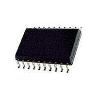
ATA3741P3-TGSY Atmel, ATA3741P3-TGSY Datasheet - Page 17

ATA3741P3-TGSY
Manufacturer Part Number
ATA3741P3-TGSY
Description
RF Receiver ASK/FSK Rem. Ctrl. Rec. (IF= 600 kHz)
Manufacturer
Atmel
Type
Receiverr
Datasheet
1.ATA3741P2-TGSY.pdf
(31 pages)
Specifications of ATA3741P3-TGSY
Package / Case
SOIC-20
Operating Frequency
450 MHz
Operating Supply Voltage
5 V
Maximum Operating Temperature
+ 105 C
Minimum Operating Temperature
- 40 C
Mounting Style
SMD/SMT
Operating Frequency (max)
450000kHz
Operating Temperature (min)
-40C
Operating Temperature (max)
105C
Operating Temperature Classification
Industrial
Operating Supply Voltage (min)
4.5V
Operating Supply Voltage (typ)
5V
Operating Supply Voltage (max)
5.5V
Lead Free Status / RoHS Status
Lead free / RoHS Compliant
Figure 5-11. Timing Diagram of the OFF Command Via Pin DATA
Figure 5-12. Timing Diagram of the OFF Command Via Pin ENABLE
5.5
4899B–RKE–10/06
Configuration of the Receiver
DATA (U3741BM)
Serial bi-directional
data line
Out1 (microcontroller)
ENABLE
DATA (U3741BM)
Serial bi-directional
data line
Receiver
The ATA3741 receiver is configured via two 12-bit RAM registers called OPMODE and LIMIT.
The registers can be programmed by means of the bi-directional DATA port. If the register con-
tents have changed due to a voltage drop, this condition is indicated by a certain output pattern
called reset marker (RM). The receiver must be reprogrammed in that case. After a power-on
reset (POR), the registers are set to default mode. If the receiver is operated in default mode,
there is no need to program the registers.
Table 5-2 on page 18
the receiver is set back to polling mode via the OFF command, (see Section
on page
ate register to be programmed.
Table 5-1.
X
on
X
X
X
Receiver on
Bit 1
1
0
0
t1
15) or if it is programmed. Bit 2 represents the register address; it selects the appropri-
OFF command
Effect of Bit 1 and Bit 2 in Programming the Registers
t
off
t2
T
Doze
t3
shows the structure of the registers. As shown in
Bit 2
(Start bit)
x
1
0
t4
Bit 1
("1")
t10
t7
t5
Action
The receiver is set back to polling mode (OFF command)
The OPMODE register is programmed
The LIMIT register is programmed
T
Sleep
T
Sleep
Startup mode
X
X
Table
Startup mode
5-1, bit 1 defines if
“Receiving Mode”
ATA3741
X
X
17


