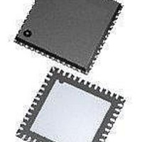
MAX2369EGM+TD Maxim Integrated Products, MAX2369EGM+TD Datasheet - Page 15

MAX2369EGM+TD
Manufacturer Part Number
MAX2369EGM+TD
Description
RF Transmitter Complete Dual-Band Q uadrature Transmitte
Manufacturer
Maxim Integrated Products
Type
Complete Dual-Band Quadrature Transmitterr
Datasheet
1.MAX2369EGMTD.pdf
(16 pages)
Specifications of MAX2369EGM+TD
Package / Case
QFN-48
Operating Frequency
120 MHz to 235 MHz
Maximum Operating Temperature
+ 85 C
Mounting Style
SMD/SMT
Noise Figure
- 145 dBm/Hz
Operating Supply Voltage
2.7 V to 3 V
Supply Current
80 mA to 155 mA
Supply Voltage (max)
5.5 V
Supply Voltage (min)
2.7 V
Lead Free Status / RoHS Status
Lead free / RoHS Compliant
The IF VCO tank (TANK+, TANK-) is fully differential.
The external tank components are shown in
The frequency of oscillation is determined by the follow-
ing equation:
C
C
C
C
and traces
C
quency
C
Figure 3. 3-Wire Interface Diagram
Figure 4. Tank Port Oscillator
C
f
OSC
INT
D
VAR
PAR
CENT
C
VAR
= Capacitance of varactor
= External coupling capacitor to the varactor
= Internal capacitance of TANK port
C
C
= Equivalent variable tuning capacitance
D
D
= Parasitic capacitance due to PC board pads
=
= External capacitor for centering oscillation fre-
NOTE: THE 3-WIRE BUS IS SPI/QSPI/MICROWIRE-COMPATIBLE.
=
2
C
C
C
π
C
C
2 (C
CENT
C
D
(C
D
INT
×
______________________________________________________________________________________
+ C )
CLK
CS
C
DI
L
C
+
C
C
B19 (MSB)
C
CENT
PAR
1
+
t
CS
B18
C
IF Tank Design
C
INT
VAR
MAX2369
+
-R
n
C
Figure
PAR
) L
B0
t
4.
CH
Quadrature Transmitter
A3
Internal to the IC, the charge pump will have a leakage
of less than 10nA. This is equivalent to a 300MΩ shunt
resistor. The charge-pump output must see an
extremely high DC resistance of greater than 300MΩ.
This will minimize charge-pump spurs at the compari-
son frequency. Make sure there is no solder flux under
the varactor or loop filter.
The MAX2369 EV kit can be used as a starting point for
layout. For best performance, take into consideration
power-supply issues, as well as the RF, LO, and IF lay-
out.
To minimize coupling between different sections of the
IC, the ideal power-supply layout is a star configuration,
which has a large decoupling capacitor at a central
V
each going to a separate V
circuit. At the end of each trace is a bypass capacitor
with impedance to ground less than 1Ω at the frequen-
cy of interest. This arrangement provides local decou-
pling at each V
capacitor for a low-inductance ground connection.
The layout of a matching network can be very sensitive
to parasitic circuit elements. To minimize parasitic
inductance, keep all traces short and place compo-
nents as close to the IC as possible. To minimize para-
sitic capacitance, a cutout in the ground plane (and
any other planes) below the matching network compo-
nents can be used.
On the high-impedance ports (e.g., IF inputs and out-
puts), keep traces short to minimize shunt capacitance.
t
CC
CWL
t
node. The V
CWH
Complete Dual-Band
CC
A1
CC
pin. Use at least one via per bypass
traces branch out from this node,
Matching Network Layout
A0 (LSB)
t
ES
Power-Supply Layout
CC
t
EW
node in the MAX2369
Layout Issues
t
t
t
t
t
t
CS
CH
CWH
ES
CWL
EW
> 50ns
> 50ns
> 10ns
> 50ns
> 50ns
> 50ns
15


