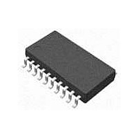
U2793B-NFSG3H19 Atmel, U2793B-NFSG3H19 Datasheet - Page 4

U2793B-NFSG3H19
Manufacturer Part Number
U2793B-NFSG3H19
Description
Modulator / Demodulator Com.Cellular 300MHz
Manufacturer
Atmel
Datasheet
1.DEMOBOARD-U2793B.pdf
(13 pages)
Specifications of U2793B-NFSG3H19
Package / Case
SSO-20
Maximum Operating Temperature
+ 125 C
Minimum Operating Temperature
- 55 C
Modulation Type
Quadrature
Mounting Style
SMD/SMT
Operating Supply Voltage
5 V
Supply Current
15 mA
3. Absolute Maximum Ratings
Stresses beyond those listed under “Absolute Maximum Ratings” may cause permanent damage to the device. This is a stress rating
only and functional operation of the device at these or any other conditions beyond those indicated in the operational sections of this
specification is not implied. Exposure to absolute maximum rating conditions for extended periods may affect device reliability.
4. Thermal Resistance
5. Operating Range
6. Electrical Characteristics
Test conditions (unless otherwise specified); V
System impedance Zo = 50 , f
4
No.
Notes:
Parameters
Supply voltage
Input voltage
Junction temperature
Storage temperature range
Parameters
Junction ambient SSO20
Parameters
Supply voltage
Ambient temperature range
1.1
1.2
2.1
2.2
2.3
2.4
3.1
3.2
3.3
3.4
3.5
2
3
Parameters
Supply voltage range
Supply current
Baseband Inputs, Pin 9-10, 11-12
Input-voltage range (differential)
Input impedance
Input-frequency range
Input voltage, common mode
LO Input, Pins 14 and 15
Frequency range
Input level
Input impedance
Voltage standing wave ratio
Duty-cycle range
1. Required LO level is a function of the LO frequency.
2. The LO input impedance is consisting of a 50
3. With the pins 19 and 20 spurious performance especially for low frequency application can be improved by adding a chip
4. For T
U2793B
capacitor between LP1 and LP2. In conjunction with a parallel resistor the output level can be adjusted to the following
mixer stage without degration of LO suppression and noise performance which would decrease if the I/Q input level is
reduced.
(1)
amb
= –40°C to +85°C and V
LO
=150 MHz, P
Test Conditions
S
S
LO
= 5V, T
= 4.5V to 5.5V
= -15 dBm, V
amb
Symbol
Symbol
Symbol
= 25°C, referred to test circuit.
R
T
T
V
V
V
T
amb
thJA
Stg
S
S
resistor in series with a 15 pF capacitor.
j
i
BBi
= 1.0 V
6, 7
6, 7
Pin
pp
, differential
VSWR
Symbol
DCR
V
P
Z
Z
f
f
V
I
BBi
LOi
BBi
iLO
BBi
LOi
S
S
LO
–55 to +125
LO
–40 to +85
4.5 to 5.5
0 to V
Value
Value
Value
125
140
6
Min.
4.5
0.4
30
0
S
1000
Typ.
–15
2.5
3.5
(2)
15
30
5
Max.
1500
300
5.5
0.6
50
–5
mVpp
4651E–CELL–07/06
MHz
MHz
dBm
Unit
mA
k
V
V
Unit
Unit
Unit
K/W
°C
°C
°C
V
V
V
Type*
A
A
D
D
D
D
D
D
D
D


