NJM1496V-TE1 NJR, NJM1496V-TE1 Datasheet
NJM1496V-TE1
Specifications of NJM1496V-TE1


Related parts for NJM1496V-TE1


NJM1496V-TE1 Summary of contents
Page 1
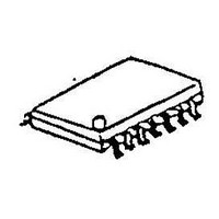
... High Common Mode Rejection 85dB Typ. ● Package Outline DIP14, DMP14, SSOP14 ● Bipolar Technology ■ APPLICATION ● Balanced Modulation ● Synchronous Detection ● FM Detection ● Phase Detection ● Sampling ■ PIN CONFIGURATION ■ EQUIVALENT CIRCUIT Ver.2003-12-09 ■ PACKAGE OUTLINE NJM1496D NJM1496M NJM1496V NJM1496D NJM1496M NJM1496V - 1 - ...
Page 2
ABSOLUTE MAXIMUM RATINGS PARAMETER Applied Voltage 30 (Applied Pins 6-8, 12-8, 6-10, 12-10, 10-1, 8-1, 10-4, 8-4, 2-5, 3-5) Carrier Input Voltage Signal Input Voltage Input Signal Bias Current ( Power Dissipation Operating Temperature Range Storage Temperature ...
Page 3
ELECTRICAL CHARACTERISTICS PARAMETER Carrier Feedthrough Carrier Suppression Transadmittance Bandwidth (R =50Ω) L Carrier Input Port Signal Input Port Voltage Gain, Signal Channel Signal Port Common Mode Input Voltage Range Signal Port Common Mode Rejection Ratio Differential Output Swing Capability ...
Page 4
TYPICAL CHARACTERISTICS Carrier Suppression Carrier Feedthrough - 4 - Carrier Suppression Sideband Output Ver.2003-12-09 ...
Page 5
TYPICAL APPLICATIONS AM Modulator Circuit Product Detector (+12V DC Single Supply) Ver.2003-12-09 [CAUTION] The specifications on this databook are only given for information , without any guarantee as regards either mistakes or omissions. The application circuits in this databook ...