Product Features
•
•
•
•
•
•
•
•
Applications
•
Specifications
1. Test conditions unless otherwise noted: 25ºC, Vdd = +5 V in a tuned application circuit. Vctrl is the control voltage through a BJT transistor and a 100 Ω dropping resistor as shown in the same application circuit.
2. 3OIP measured with two tones at an output power of +5 dBm/tone separated by 10 MHz. The suppression on the largest IM3 product is used to calculate the 3OIP using a 2:1 rule.
3. The gain variation range is measured as the difference in gain with Vctrl = 0V and Vctrl = 4.5V at 0.9 GHz.
Absolute Maximum Rating
Operation of this device above any of these parameters may cause permanent damage.
TriQuint Semiconductor, Inc •
VG101
Cellular-band Variable Gain Amplifier
Parameter
Operational Bandwidth
Test Frequency
Gain at min. attenuation
Input Return Loss
Output Return Loss
Output P1dB
Output IP3
Noise Figure at min. attenuation
Gain Variation Range
Gain Variation Control Voltage, V
Group Delay
Supply Voltage
Operating Amplifier Current Range
Gain Control Pin Current
Parameter
Operating Case Temperature
Storage Temperature
Amplifier Supply Voltage (pin 25)
Pin 5 (Gain Control) Current
RF Input Power (continuous)
Junction Temperature
Thermal Resistance, Rth
700 – 1000 MHz bandwidth
28 dB Attenuation Range
+40 dBm Output IP3
+22 dBm P1dB
Constant IP3 & P1dB over
attenuation range
Single voltage supply
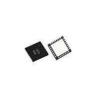
Pb-free 6mm 28-pin QFN package
MTTF > 1000 years
Xmit & Rcv AGC circuitry for
mobile infrastructure
(1)
(1)
Phone +1-503-615-9000 • FAX: +1-503-615-8900
CTRL
Rating
-40 to +85 °C
-55 to +125 °C
+6 V
30 mA
+12 dBm
+160 °C
59 °C / W
The VG101 is a cellular-band high dynamic range
variable gain amplifier (VGA) packaged in a low
profile Pb-free / RoHS-compliant surface-mount
leadless package that measures 6 x 6 mm square.
The +22 dBm output compression point and +40
dBm output intercept point of the amplifier are
maintained over the entire attenuation range, making
the VG101 ideal for use in transmitter and receiver
AGC circuits and as a variable gain stage following
an LNA in high dynamic range receiver front ends.
Superior thermal design allows the product to have a
minimum MTTF rating of 1000 years at a mounting
temperature of +85 ºC. All devices are 100% RF &
DC tested and packaged on tape and reel for
automated surface-mount assembly.
Units
MHz
MHz
dBm
dBm
mA
mA
dB
dB
dB
dB
dB
ns
V
V
Product Description
Min
25.5
+37
700
120
15
0
• e-mail: info-sales@tqs.com • Web site: www.TriQuint.com
Ordering Information
Standard tape / reel size = 500 pieces on a 7″ reel
Typ
28.7
+22
+40
Part No.
VG101-F
VG101-PCB
900
150
3.5
12
14
+5
16
1
Max
1000
33.5
180
4.5
20
Specifications and information are subject to change without notice
Description
Cellular-band Variable Gain Amplifier
(lead-free/RoHS-compliant QFN package)
Fully Assembled Application Board
See note 1
See note 2
V
See note 3
See note 1
Frequency = 900 MHz
Pin 25
V
CTRL
CTRL
Functional Diagram
= 0 V
= 4.5 V. See note 1.
RF IN
GND
GND
GND
GND
GND
GND
10
11
12
13
14
8
9
Conditions
15
7
Attenuator
Variable
16
6
17
5
Page 1 of 4
18
4
19
3
Amp
20
2
21
August 2009
1
28
27
26
25
24
23
22
GND
GND
GND
RF OUT
GND
GND
GND