MJD3055G ON Semiconductor, MJD3055G Datasheet

TRANS POWER NPN 10A 60V DPAK

MJD3055G

Manufacturer Part Number
MJD3055G
Description
TRANS POWER NPN 10A 60V DPAK
Manufacturer
ON Semiconductor
Type
Powerr
Datasheets

Specifications of MJD3055G

Transistor Type
NPN
Current - Collector (ic) (max)
10A
Voltage - Collector Emitter Breakdown (max)
60V
Vce Saturation (max) @ Ib, Ic
8V @ 3.3A, 10A
Current - Collector Cutoff (max)
50µA
Dc Current Gain (hfe) (min) @ Ic, Vce
20 @ 4A, 4V
Power - Max
1.75W
Frequency - Transition
2MHz
Mounting Type
Surface Mount
Package / Case
DPak, TO-252 (2 leads+tab), SC-63
Configuration
Single
Transistor Polarity
NPN
Mounting Style
SMD/SMT
Collector- Emitter Voltage Vceo Max
60 V
Emitter- Base Voltage Vebo
5 V
Continuous Collector Current
10 A
Maximum Dc Collector Current
10 A
Power Dissipation
20 W
Maximum Operating Frequency
2 MHz
Maximum Operating Temperature
+ 150 C
Dc Collector/base Gain Hfe Min
20 at 4 A at 4 V
Minimum Operating Temperature
- 55 C
Current, Collector
10 A
Current, Gain
5
Frequency
2 MHz
Package Type
DPAK
Polarity
NPN
Primary Type
Si
Resistance, Thermal, Junction To Case
6.25 °C/W
Voltage, Breakdown, Collector To Emitter
60 V
Voltage, Collector To Base
70 V
Voltage, Collector To Emitter
60 V
Voltage, Collector To Emitter, Saturation
8 V
Voltage, Emitter To Base
5 V
Lead Free Status / RoHS Status
Lead free / RoHS Compliant
Other names
MJD3055G
MJD3055GOS

Available stocks

Company
Part Number
Manufacturer
Quantity
Price
Part Number:
MJD3055G
Manufacturer:
ON
Quantity:
12 500
Part Number:
MJD3055G
Manufacturer:
ON/安森美
Quantity:
20 000
MJD2955 (PNP)
MJD3055 (NPN)
Complementary Power
Transistors
DPAK For Surface Mount Applications
applications.
Features
Maximum ratings are those values beyond which device damage can occur.
Maximum ratings applied to the device are individual stress limit values (not
normal operating conditions) and are not valid simultaneously. If these limits are
exceeded, device functional operation is not implied, damage may occur and
reliability may be affected.
†Safe Area Curves are indicated by Figure 1. Both limits are applicable and must
1. These ratings are applicable when surface mounted on the minimum pad
MAXIMUM RATINGS
THERMAL CHARACTERISTICS
Collector−Emitter Voltage
Collector−Base Voltage
Emitter−Base Voltage
Collector Current
Base Current
Total Power Dissipation @ T
Derate above 25°C
Total Power Dissipation (Note1)
Operating and Storage Junction
Temperature Range
Thermal Resistance, Junction−to−Case
Thermal Resistance, Junction−to−Ambient
(Note1)
be observed.
Designed for general purpose amplifier and low speed switching
(No Suffix)
Lead Formed for Surface Mount Applications in Plastic Sleeves
Straight Lead Version in Plastic Sleeves (“−1” Suffix)
Electrically Similar to MJE2955 and MJE3055
DC Current Gain Specified to 10 Amperes
High Current Gain−Bandwidth Product − f
Epoxy Meets UL 94 V−0 @ 0.125 in
ESD Ratings: Human Body Model, 3B u 8000 V
Pb−Free Packages are Available
sizes recommended.
@ T
Derate above 25°C
Characteristic
A
= 25°C
Rating
Machine Model, C u 400 V
C
= 25°C
Symbol
Symbol
T
V
R
J
R
P
V
V
P
, T
CEO
I
I
qJC
qJA
CB
EB
D
C
B
D
T
{
stg
= 2.0 MHz (Min) @ I
= 500 mAdc
−55 to +150
0.014
Max
0.16
1.75
Max
6.25
71.4
60
70
10
20
5
6
1
W/°C
W/°C
°C/W
°C/W
Unit
Unit
Vdc
Vdc
Vdc
Adc
Adc
°C
W
W
C
See detailed ordering and shipping information in the package
dimensions section on page 2 of this data sheet.
1 2
1
POWER TRANSISTORS
2
60 VOLTS, 20 WATTS
3
3
ORDERING INFORMATION
Y
WW
Jxx55 = Device Code
G
4
10 AMPERES
4
CASE 369C
CASE 369D
STYLE 1
STYLE 1
DPAK−3
SILICON
DPAK
= Year
= Work Week
= Pb−Free Package
x = 29 or 30
DIAGRAMS
MARKING
xx55G
YWW
xx55G
YWW
J
J

Related parts for MJD3055G

MJD3055G Summary of contents

Page 1

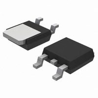
MJD2955 (PNP) MJD3055 (NPN) Complementary Power Transistors DPAK For Surface Mount Applications Designed for general purpose amplifier and low speed switching applications. Features • Lead Formed for Surface Mount Applications in Plastic Sleeves (No Suffix) • Straight Lead Version in ...

Page 2

... MJD2955 MJD2955G MJD2955−001 MJD2955−001G MJD2955T4 MJD2955T4G MJD3055 MJD3055G MJD3055T4 MJD3055T4G †For information on tape and reel specifications, including part orientation and tape sizes, please refer to our Tape and Reel Packaging Specifications Brochure, BRD8011/D. MJD2955 (PNP) MJD3055 (NPN 25_C unless otherwise noted) ...

Page 3

... 0.13 (0.005) M 5.80 0.228 *For additional information on our Pb−Free strategy and soldering details, please download the ON Semiconductor Soldering and Mounting Techniques Reference Manual, SOLDERRM/D. PACKAGE DIMENSIONS DPAK CASE 369C−01 ISSUE O SEATING −T− PLANE SOLDERING FOOTPRINT* 6.20 3.0 0.244 0.118 2 ...

Page 4

MJD2955 (PNP) MJD3055 (NPN −T− SEATING K PLANE 0.13 (0.005) M PACKAGE DIMENSIONS DPAK−3 CASE 369D−01 ISSUE B C NOTES ...

Related keywords