2N4918G ON Semiconductor, 2N4918G Datasheet
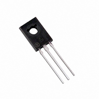
TRANS PNP GP 1A 40V TO225AA

2N4918G

Manufacturer Part Number
2N4918G
Description
TRANS PNP GP 1A 40V TO225AA
Manufacturer
ON Semiconductor
Type
Medium Powerr
Datasheets

Specifications of 2N4918G

Transistor Type
PNP
Current - Collector (ic) (max)
1A
Voltage - Collector Emitter Breakdown (max)
40V
Vce Saturation (max) @ Ib, Ic
600mV @ 100mA, 1A
Current - Collector Cutoff (max)
500µA
Dc Current Gain (hfe) (min) @ Ic, Vce
30 @ 500mA, 1V
Power - Max
30W
Frequency - Transition
3MHz
Mounting Type
Through Hole
Package / Case
TO-225-3
Transistor Polarity
PNP
Mounting Style
Through Hole
Collector- Emitter Voltage Vceo Max
40 V
Emitter- Base Voltage Vebo
5 V
Maximum Dc Collector Current
3 A
Power Dissipation
30 W
Maximum Operating Temperature
+ 150 C
Continuous Collector Current
3 A
Dc Collector/base Gain Hfe Min
40
Maximum Operating Frequency
3 MHz
Minimum Operating Temperature
- 65 C
Current, Collector
1 A
Current, Gain
10
Frequency
3 MHz
Package Type
TO-225
Polarity
PNP
Primary Type
Si
Resistance, Thermal, Junction To Case
4.16 °C/W
Voltage, Breakdown, Collector To Emitter
40 V
Voltage, Collector To Base
40 V
Voltage, Collector To Emitter
40 V
Voltage, Collector To Emitter, Saturation
0.6 V
Voltage, Emitter To Base
5 V
Number Of Elements
1
Collector-emitter Voltage
40V
Collector-base Voltage
40V
Emitter-base Voltage
5V
Collector Current (dc) (max)
3A
Dc Current Gain (min)
40
Frequency (max)
3MHz
Operating Temp Range
-65C to 150C
Operating Temperature Classification
Military
Mounting
Through Hole
Pin Count
3
Lead Free Status / RoHS Status
Lead free / RoHS Compliant
Other names
2N4918GOS

Available stocks

Company
Part Number
Manufacturer
Quantity
Price
Part Number:
2N4918G
Manufacturer:
ON
Quantity:
2 395
Part Number:
2N4918G
Manufacturer:
ON Semiconductor
Quantity:
2
Î Î Î Î Î Î Î Î Î Î Î Î Î Î Î Î Î Î Î Î Î Î Î
Î Î Î Î Î Î Î Î Î Î Î
Î Î Î Î Î Î Î Î Î Î Î Î Î Î Î Î Î Î Î Î Î Î Î
Î Î Î Î Î Î Î Î Î Î Î
Î Î Î Î Î Î Î Î Î Î Î Î Î Î Î Î Î Î Î Î Î Î Î
Î Î Î Î Î Î Î Î Î Î Î Î
applications. These high–performance plastic devices feature:
*Indicates JEDEC Registered Data for 2N4918 Series.
(1) The 1.0 Amp maximum I C value is based upon JEDEC current gain requirements.
(2) Recommend use of thermal compound for lowest thermal resistance.
Preferred devices are ON Semiconductor recommended choices for future use and best overall value.
*MAXIMUM RATINGS
THERMAL CHARACTERISTICS (2)
April, 2002 – Rev. 10
Collector–Emitter Voltage
Collector–Base Voltage
Emitter–Base Voltage
Collector Current — Continuous (1)
Base Current
Total Power Dissipation @ T C = 25 C
Operating & Storage Junction
Thermal Resistance, Junction to Case
. . . designed for driver circuits, switching, and amplifier
Low Saturation Voltage —
Excellent Power Dissipation Due to Thermopad Construction —
Excellent Safe Operating Area
Gain Specified to I C = 1.0 Amp
Complement to NPN 2N4921, 2N4922, 2N4923
Semiconductor Components Industries, LLC, 2002
The 3.0 Amp maximum value is based upon actual current–handling capability of the
device (See Figure 5).
Derate above 25_C
Temperature Range
V CE(sat) = 0.6 Vdc (Max) @ I C = 1.0 Amp
P D = 30 W @ T C = 25_C
Characteristic
Ratings
)
Î Î Î
Î Î Î
Î Î Î
Î Î Î
Î Î Î
Î Î Î
Î Î Î
Î Î Î
Î Î Î
Î Î Î
Î Î Î
Î Î Î
Î Î Î
Î Î Î
Î Î Î
Î Î Î
Î Î Î
Î Î Î
Symbol
T J , T stg
V CEO
Î Î Î Î Î
Î Î Î Î Î
Î Î Î Î Î
Î Î Î Î Î
V CB
V EB
I C *
P D
I B
Î Î Î Î Î Î Î Î Î
Î Î Î Î Î Î Î Î Î
Î Î Î Î
Î Î Î Î
Î Î Î Î
Î Î Î Î
Î Î Î Î
Î Î Î Î
Î Î Î Î Î Î Î Î Î
Î Î Î Î Î Î Î Î Î
Î Î Î Î Î Î Î Î Î
Î Î Î Î Î Î Î Î Î
Î Î Î Î Î Î Î Î Î
Î Î Î Î Î Î Î Î Î
Î Î Î Î Î Î Î Î Î
Î Î Î Î Î Î Î Î Î
Î Î Î Î Î Î Î Î Î
Î Î Î Î Î Î Î Î Î
Symbol
2N4918
JC
40
40
Î Î Î
Î Î Î
Î Î Î
Î Î Î
Î Î Î
Î Î Î
Î Î Î Î Î Î
Î Î Î Î Î Î
Î Î Î Î Î Î
Î Î Î Î Î Î
–65 to +150
2N4919
0.24
5.0
1.0
3.0
1.0
60
60
30
1
Î Î Î Î
Î Î Î Î
Î Î Î Î
Î Î Î Î
Î Î Î Î
Î Î Î Î
Max
4.16
2N4920
80
80
Î Î Î
Î Î Î
Î Î Î
Î Î Î
Î Î Î
Î Î Î
Î Î Î
Î Î Î
Î Î Î
Î Î Î
Î Î Î
Î Î Î
Î Î Î
Î Î Î
Î Î Î
Î Î Î
Î Î Î
Î Î Î
Î Î Î
Î Î Î
Î Î Î
Î Î Î
_C/W
Watts
W/_C
Unit
Unit
Vdc
Vdc
Vdc
Adc
Adc
_C
*ON Semiconductor Preferred Device
POWER TRANSISTORS
GENERAL–PURPOSE
3 2
Publication Order Number:
TO–225AA TYPE
1
40–80 VOLTS
CASE 77–09
3 AMPERE
30 WATTS
2N4918/D

Related parts for 2N4918G

2N4918G Summary of contents

Page 1

... The 3.0 Amp maximum value is based upon actual current–handling capability of the device (See Figure 5). (2) Recommend use of thermal compound for lowest thermal resistance. Preferred devices are ON Semiconductor recommended choices for future use and best overall value. Semiconductor Components Industries, LLC, 2002 April, 2002 – Rev. 10 Î ...

Page 2

Figure 1. Power Derating http://onsemi.com 2 ...

Page 3

ELECTRICAL CHARACTERISTICS Î Î Î Î Î ...

Page 4

Figure 5. Active–Region Safe Operating Area Figure 6. Storage Time 2N4918 thru 2N4920 Figure 4. Thermal Response There are two limitations on the power handling ability of a transistor: average junction temperature and second breakdown. Safe operating area curves indicate ...

Page 5

TYPICAL DC CHARACTERISTICS Figure 8. Current Gain Figure 10. Effects of Base–Emitter Resistance Figure 12. Collector Cut–Off Region 2N4918 thru 2N4920 Figure 9. Collector Saturation Region Figure 11. “On” Voltage Figure 13. Temperature Coefficients http://onsemi.com 5 + ...

Page 6

PACKAGE DIMENSIONS TO–225AA CASE 77–09 ISSUE W –B– –A– http://onsemi.com ...

Page 7

Notes 2N4918 thru 2N4920 http://onsemi.com 7 ...

Page 8

... Fax: 303–675–2176 or 800–344–3867 Toll Free USA/Canada Email: ONlit@hibbertco.com N. American Technical Support: 800–282–9855 Toll Free USA/Canada 2N4918 thru 2N4920 JAPAN: ON Semiconductor, Japan Customer Focus Center 4–32–1 Nishi–Gotanda, Shinagawa–ku, Tokyo, Japan 141–0031 Phone: 81–3–5740–2700 Email: r14525@onsemi.com ON Semiconductor Website: http://onsemi ...

Related keywords