TIP120-BP Micro Commercial Components (MCC), TIP120-BP Datasheet
TIP120-BP
Specifications of TIP120-BP


Related parts for TIP120-BP

TIP120-BP Summary of contents
Page 1
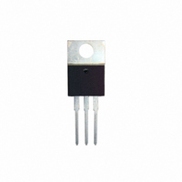
... O 62.5 C/W C Unless Otherwise Specified O Min Max Units 60 --- Vdc --- 0.2 mAdc --- 2.0 mAdc --- 0.5 mAdc 1000 --- 1000 --- --- 2.0 Vdc --- 4.0 Vdc --- 2.5 Vdc TIP120 NPN Epitaxial Darlington Transistors TO-220 PIN 1. BASE N PIN 2. COLLECTOR PIN 3. EMITTER DIMENSIONS INCHES MM MIN MAX DIM MIN ...
Page 2
... MCC's products are not authorized for use as critical components in life support devices or systems without the express written Counterfeiting of semiconductor parts is a growing problem in the industry. Micro Commercial Components (MCC) is taking strong measures to protect ourselves and our customers from the proliferation of counterfeit parts. MCC strongly encourages customers to purchase MCC parts either directly from MCC or from Authorized MCC Distributors who are listed by country on our web page cited below ...