MJ14002G ON Semiconductor, MJ14002G Datasheet - Page 2
MJ14002G
Manufacturer Part Number
MJ14002G
Description
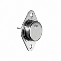
TRANS PWR NPN 60A 80V TO3
Manufacturer
ON Semiconductor
Type
High Current, Powerr
Specifications of MJ14002G
Transistor Type
NPN
Current - Collector (ic) (max)
60A
Voltage - Collector Emitter Breakdown (max)
80V
Vce Saturation (max) @ Ib, Ic
3V @ 12A, 60A
Current - Collector Cutoff (max)
1mA
Dc Current Gain (hfe) (min) @ Ic, Vce
15 @ 50A, 3V
Power - Max
300W
Mounting Type
Chassis Mount
Package / Case
TO-204, TO-3
Transistor Polarity
NPN
Mounting Style
SMD/SMT
Collector- Emitter Voltage Vceo Max
80 V
Emitter- Base Voltage Vebo
5 V
Maximum Dc Collector Current
60 A
Power Dissipation
300 W
Maximum Operating Temperature
+ 200 C
Continuous Collector Current
60 A
Dc Collector/base Gain Hfe Min
30
Minimum Operating Temperature
- 65 C
Current, Collector
60 A
Current, Gain
5
Package Type
TO-204 (TO-3)
Polarity
NPN
Primary Type
Si
Resistance, Thermal, Junction To Case
0.584 °C/W
Voltage, Breakdown, Collector To Emitter
80 V
Voltage, Collector To Base
80 V
Voltage, Collector To Emitter
80 V
Voltage, Collector To Emitter, Saturation
3 V
Voltage, Emitter To Base
5 V
Lead Free Status / RoHS Status
Lead free / RoHS Compliant
Frequency - Transition
-
Lead Free Status / Rohs Status
Lead free / RoHS Compliant
Other names
MJ14002GOS
Available stocks
Company
Part Number
Manufacturer
Quantity
Price
Company:

Part Number:
MJ14002G
Manufacturer:
ST
Quantity:
1 929
Part Number:
MJ14002G
Manufacturer:
ON/安森美
Quantity:
20 000


Î Î Î Î Î Î Î Î Î Î Î Î Î Î Î Î Î Î Î Î Î Î Î Î Î Î Î Î Î Î Î Î Î
Î Î Î Î Î Î Î Î Î Î Î Î Î Î Î Î Î Î Î Î Î Î Î Î Î Î Î Î Î Î Î Î Î
Î Î Î Î Î Î Î Î Î Î Î Î Î Î Î Î Î Î Î Î Î Î Î
Î Î Î Î Î Î Î Î Î Î Î Î Î Î Î Î Î Î Î Î Î Î Î
Î Î Î Î Î Î Î Î Î Î Î Î Î Î Î Î Î Î Î Î Î Î Î
Î Î Î Î Î Î Î Î Î Î Î Î Î Î Î Î Î Î Î Î Î Î Î
Î Î Î Î Î Î Î Î Î Î Î Î Î Î Î Î Î Î Î Î Î Î Î Î Î Î Î Î Î Î Î Î Î
Î Î Î Î Î Î Î Î Î Î Î Î Î Î Î Î Î Î Î Î Î Î Î Î Î Î Î Î Î Î Î Î Î
Î Î Î Î Î Î Î Î Î Î Î Î Î Î Î Î Î Î Î Î Î Î Î
Î Î Î Î Î Î Î Î Î Î Î Î Î Î Î Î Î Î Î Î Î Î Î
Î Î Î Î Î Î Î Î Î Î Î Î Î Î Î Î Î Î Î Î Î Î Î Î Î Î Î Î Î Î Î Î Î
Î Î Î Î Î Î Î Î Î Î Î Î Î Î Î Î Î Î Î Î Î Î Î Î Î Î Î Î Î Î Î Î Î
Î Î Î Î Î Î Î Î Î Î Î Î Î Î Î Î Î Î Î Î Î Î Î
Î Î Î Î Î Î Î Î Î Î Î Î Î Î Î Î Î Î Î Î Î Î Î
Î Î Î Î Î Î Î Î Î Î Î Î Î Î Î Î Î Î Î Î Î Î Î
Î Î Î Î Î Î Î Î Î Î Î Î Î Î Î Î Î Î Î Î Î Î Î
Î Î Î Î Î Î Î Î Î Î Î Î Î Î Î Î Î Î Î Î Î Î Î
Î Î Î Î Î Î Î Î Î Î Î Î Î Î Î Î Î Î Î Î Î Î Î
Î Î Î Î Î Î Î Î Î Î Î Î Î Î Î Î Î Î Î Î Î Î Î
Î Î Î Î Î Î Î Î Î Î Î Î Î Î Î Î Î Î Î Î Î Î Î
Î Î Î Î Î Î Î Î Î Î Î Î Î Î Î Î Î Î Î Î Î Î Î
Î Î Î Î Î Î Î Î Î Î Î Î Î Î Î Î Î Î Î Î Î Î Î
Î Î Î Î Î Î Î Î Î Î Î Î Î Î Î Î Î Î Î Î Î Î Î
Î Î Î Î Î Î Î Î Î Î Î Î Î Î Î Î Î Î Î Î Î Î Î
Î Î Î Î Î Î Î Î Î Î Î Î Î Î Î Î Î Î Î Î Î Î Î
Î Î Î Î Î Î Î Î Î Î Î Î Î Î Î Î Î Î Î Î Î Î Î
Î Î Î Î Î Î Î Î Î Î Î Î Î Î Î Î Î Î Î Î Î Î Î
Î Î Î Î Î Î Î Î Î Î Î Î Î Î Î Î Î Î Î Î Î Î Î Î Î Î Î Î Î Î Î Î Î
Î Î Î Î Î Î Î Î Î Î Î Î Î Î Î Î Î Î Î Î Î Î Î Î Î Î Î Î Î Î Î Î Î
Î Î Î Î Î Î Î Î Î Î Î Î Î Î Î Î Î Î Î Î Î Î Î
Î Î Î Î Î Î Î Î Î Î Î Î Î Î Î Î Î Î Î Î Î Î Î
Î Î Î Î Î Î Î Î Î Î Î Î Î Î Î Î Î Î Î Î Î Î Î
Î Î Î Î Î Î Î Î Î Î Î Î Î Î Î Î Î Î Î Î Î Î Î
Î Î Î Î Î Î Î Î Î Î Î Î Î Î Î Î Î Î Î Î Î Î Î
Î Î Î Î Î Î Î Î Î Î Î Î Î Î Î Î Î Î Î Î Î Î Î
Î Î Î Î Î Î Î Î Î Î Î Î Î Î Î Î Î Î Î Î Î Î Î
Î Î Î Î Î Î Î Î Î Î Î Î Î Î Î Î Î Î Î Î Î Î Î
Î Î Î Î Î Î Î Î Î Î Î Î Î Î Î Î Î Î Î Î Î Î Î
Î Î Î Î Î Î Î Î Î Î Î Î Î Î Î Î Î Î Î Î Î Î Î
Î Î Î Î Î Î Î Î Î Î Î Î Î Î Î Î Î Î Î Î Î Î Î
Î Î Î Î Î Î Î Î Î Î Î Î Î Î Î Î Î Î Î Î Î Î Î Î Î Î Î Î Î Î Î Î Î
Î Î Î Î Î Î Î Î Î Î Î Î Î Î Î Î Î Î Î Î Î Î Î Î Î Î Î Î Î Î Î Î Î
Î Î Î Î Î Î Î Î Î Î Î Î Î Î Î Î Î Î Î Î Î Î Î
Î Î Î Î Î Î Î Î Î Î Î Î Î Î Î Î Î Î Î Î Î Î Î
Î Î Î Î Î Î Î Î Î Î Î Î Î Î Î Î Î Î Î Î Î Î Î
1. Pulse Test: Pulse Width v 300 ms, Duty Cycle v 2.0%.
THERMAL CHARACTERISTICS
ELECTRICAL CHARACTERISTICS
OFF CHARACTERISTICS
ON CHARACTERISTICS
DYNAMIC CHARACTERISTICS
Thermal Resistance, Junction−to−Case
Collector−Emitter Sustaining Voltage (Note 1)
Collector Cutoff Current
Collector Cutoff Current
Collector Cutoff Current
Emitter Cutoff Current
DC Current Gain (Note 1)
Collector−Emitter Saturation Voltage (Note 1)
Base−Emitter Saturation Voltage (Note 1)
Output Capacitance
100
7.0
5.0
3.0
2.0
1.0
0.7
0.5
0.3
0.2
0.1
70
50
30
20
10
1.0
(I
(V
(V
(V
(V
(V
(V
(V
(I
(I
(I
(I
(I
(I
(I
(I
(I
(V
T
C
C
C
C
C
C
C
C
C
C
C
CE
CE
CE
CE
CB
CB
BE
CB
Figure 2. Maximum Rated Forward Biased
= 200 mAdc, I
= 25 Adc, V
= 50 Adc, V
= 60 Adc, V
= 25 Adc, I
= 50 Adc, I
= 60 Adc, I
= 25 Adc, I
= 50 Adc, I
= 60 Adc, I
= 25°C
= 5.0 Vdc, I
= 30 Vdc, I
= 40 Vdc, I
= 60 Vdc, V
= 80 Vdc, V
= 60 Vdc, I
= 80 Vdc, I
= 10 Vdc, I
2.0 3.0
V
CE
WIRE BOND LIMIT
THERMAL LIMIT
SECOND BREAKDOWN LIMIT
, COLLECTOR−EMITTER VOLTAGE (VOLTS)
B
B
B
B
B
B
CE
CE
CE
Safe Operating Area
= 2.5 Adc)
= 5.0 Adc)
= 12 Adc)
= 2.5 Adc)
= 5.0 Adc)
= 12 Adc)
B
B
E
E
E
5.0 7.0
C
BE(off)
BE(off)
B
= 0)
= 0)
= 0)
= 0)
= 3.0 V)
= 3.0 V)
= 3.0 V)
= 0, f = 0.1 MHz)
= 0)
= 0)
MJ14001 (PNP), MJ14002* (NPN), MJ14003* (PNP)
= 1.5 V)
= 1.5 V)
10
MJ14002, MJ14003
dc
Characteristic
Characteristic
5.0 ms
(T
20
MJ14001
C
= 25_C unless otherwise noted)
30
1.0 ms
50
70
1.0 ms
100
2
MJ14002, MJ14003
MJ14402, MJ14003
MJ14002, MJ14003
MJ14002, MJ14003
a transistor: average junction temperature and second
breakdown. Safe operating area curves indicate I
limits of the transistor that must be observed for reliable
operation: i.e., the transistor must not be subjected to greater
dissipation than the curves indicate.
variable depending on conditions. Second breakdown pulse
limits are valid for duty cycles to 10% provided T
v 200_C. T
Figure 13. At high case temperatures, thermal limitations
will reduce the power that can be handled to values less than
the limitations imposed by second breakdown.
There are two limitations on the power handling ability of
The data of Figure 2 is based on T
MJ14001
MJ14001
MJ14001
MJ14001
J(pk)
Î Î Î Î
Î Î Î Î
Î Î Î Î
Î Î Î Î
Î Î Î Î
Î Î Î Î
Î Î Î Î
Î Î Î Î
Î Î Î Î
Î Î Î Î
Î Î Î Î
Î Î Î Î
Î Î Î Î
Î Î Î Î
Î Î Î Î
Î Î Î Î
Î Î Î Î
Î Î Î Î
Î Î Î Î
Î Î Î Î
Î Î Î Î
Î Î Î Î
Î Î Î Î
Î Î Î Î
Î Î Î Î
Î Î Î Î
Î Î Î Î
Î Î Î Î
Î Î Î Î
Î Î Î Î
Î Î Î Î
Î Î Î Î
Î Î Î Î
Î Î Î Î
Î Î Î Î
may be calculated from the data in
V
Symbol
Symbol
V
V
CEO(sus)
R
I
I
I
CE(sat)
BE(sat)
I
h
C
CEO
CBO
EBO
CEX
qJC
FE
ob
Î Î Î Î Î Î
Î Î Î Î Î Î
Î Î Î Î Î Î
Î Î Î Î Î Î
Î Î Î Î
Î Î Î Î
Î Î Î Î
Î Î Î Î
Î Î Î Î
Î Î Î Î
Î Î Î Î
Î Î Î Î
Î Î Î Î
Î Î Î Î
Î Î Î Î
Î Î Î Î
Î Î Î Î
Î Î Î Î
Î Î Î Î
Î Î Î Î
Î Î Î Î
Î Î Î Î
Î Î Î Î
Î Î Î Î
Î Î Î Î
Î Î Î Î
Î Î Î Î
Î Î Î Î
Î Î Î Î
Î Î Î Î
Î Î Î Î
Î Î Î Î
Î Î Î Î
Î Î Î Î
Î Î Î Î
Min
5.0
60
80
30
15
−
−
−
−
−
−
−
−
−
−
−
−
−
−
J(pk)
0.584
Max
Î Î Î
Î Î Î
Î Î Î
Î Î Î
Î Î Î
Î Î Î
Î Î Î
Î Î Î
Î Î Î
Î Î Î
Î Î Î
Î Î Î
Î Î Î
Î Î Î
Î Î Î
Î Î Î
Î Î Î
Î Î Î
Î Î Î
Î Î Î
Î Î Î
Î Î Î
Î Î Î
Î Î Î
Î Î Î
Î Î Î
Î Î Î
Î Î Î
Î Î Î
Î Î Î
Î Î Î
2000
= 200_C; T
Max
100
1.0
1.0
1.0
1.0
1.0
1.0
1.0
1.0
2.5
3.0
2.0
3.0
4.0
−
−
−
−
Î Î Î
Î Î Î
Î Î Î
Î Î Î
Î Î Î
Î Î Î
Î Î Î
Î Î Î
Î Î Î
Î Î Î
Î Î Î
Î Î Î
Î Î Î
Î Î Î
Î Î Î
Î Î Î
Î Î Î
Î Î Î
Î Î Î
Î Î Î
Î Î Î
Î Î Î
Î Î Î
Î Î Î
Î Î Î
Î Î Î
Î Î Î
Î Î Î
Î Î Î
Î Î Î
Î Î Î
Î Î Î
Î Î Î
Î Î Î
Î Î Î
C
_C/W
− V
Unit
Unit
Vdc
Vdc
Vdc
mA
mA
mA
mA
pF
−
J(pk)
C
CE
is
Related parts for MJ14002G
Image
Part Number
Description
Manufacturer
Datasheet
Request
R

Part Number:
Description:
ON Semiconductor [VOLTAGE REGULATOR]
Manufacturer:
ON Semiconductor
Datasheet:
Part Number:
Description:
357-036-542-201 CARDEDGE 36POS DL .156 BLK LOPRO
Manufacturer:
ON Semiconductor
Datasheet:
Part Number:
Description:
357-036-542-201 CARDEDGE 36POS DL .156 BLK LOPRO
Manufacturer:
ON Semiconductor
Datasheet:
Part Number:
Description:
357-036-542-201 CARDEDGE 36POS DL .156 BLK LOPRO
Manufacturer:
ON Semiconductor
Datasheet:
Part Number:
Description:
357-036-542-201 CARDEDGE 36POS DL .156 BLK LOPRO
Manufacturer:
ON Semiconductor
Datasheet:
Part Number:
Description:
357-036-542-201 CARDEDGE 36POS DL .156 BLK LOPRO
Manufacturer:
ON Semiconductor
Datasheet:
Part Number:
Description:
357-036-542-201 CARDEDGE 36POS DL .156 BLK LOPRO
Manufacturer:
ON Semiconductor
Datasheet:
Part Number:
Description:
357-036-542-201 CARDEDGE 36POS DL .156 BLK LOPRO
Manufacturer:
ON Semiconductor
Datasheet:
Part Number:
Description:
357-036-542-201 CARDEDGE 36POS DL .156 BLK LOPRO
Manufacturer:
ON Semiconductor
Datasheet:
Part Number:
Description:
357-036-542-201 CARDEDGE 36POS DL .156 BLK LOPRO
Manufacturer:
ON Semiconductor
Datasheet:
Part Number:
Description:
357-036-542-201 CARDEDGE 36POS DL .156 BLK LOPRO
Manufacturer:
ON Semiconductor
Datasheet:
Part Number:
Description:
Manufacturer:
ON Semiconductor
Datasheet:
Part Number:
Description:
Manufacturer:
ON Semiconductor
Datasheet:
Part Number:
Description:
Manufacturer:
ON Semiconductor
Datasheet: