MJW21193G ON Semiconductor, MJW21193G Datasheet

TRANS BIPO PNP 16A 250V TO247

MJW21193G

Manufacturer Part Number
MJW21193G
Description
TRANS BIPO PNP 16A 250V TO247
Manufacturer
ON Semiconductor
Datasheet

Specifications of MJW21193G

Transistor Type
PNP
Current - Collector (ic) (max)
16A
Voltage - Collector Emitter Breakdown (max)
250V
Vce Saturation (max) @ Ib, Ic
4V @ 3.2A, 16A
Current - Collector Cutoff (max)
100µA
Dc Current Gain (hfe) (min) @ Ic, Vce
20 @ 8A, 5V
Power - Max
200W
Frequency - Transition
4MHz
Mounting Type
Through Hole
Package / Case
TO-247-3 (Straight Leads), TO-247AC
Transistor Polarity
PNP
Mounting Style
Through Hole
Collector- Emitter Voltage Vceo Max
250 V
Emitter- Base Voltage Vebo
5 V
Maximum Dc Collector Current
16 A
Power Dissipation
200 W
Maximum Operating Temperature
+ 150 C
Continuous Collector Current
16 A
Dc Collector/base Gain Hfe Min
20
Maximum Operating Frequency
4 MHz
Minimum Operating Temperature
- 65 C
Lead Free Status / RoHS Status
Lead free / RoHS Compliant
Other names
MJW21193GOS

Available stocks

Company
Part Number
Manufacturer
Quantity
Price
Part Number:
MJW21193G
Manufacturer:
ON Semiconductor
Quantity:
175
MJW21193 (PNP)
MJW21194 (NPN)
Silicon Power Transistors
technology and are specifically designed for high power audio output,
disk head positioners and linear applications.
Features
Stresses exceeding Maximum Ratings may damage the device. Maximum
Ratings are stress ratings only. Functional operation above the Recommended
Operating Conditions is not implied. Extended exposure to stresses above the
Recommended Operating Conditions may affect device reliability.
1. Pulse Test: Pulse Width = 5 ms, Duty Cycle ≤ 10%.
THERMAL CHARACTERISTICS
© Semiconductor Components Industries, LLC, 2010
March, 2010 − Rev. 4
MAXIMUM RATINGS
Collector−Emitter Voltage
Collector−Base Voltage
Emitter−Base Voltage
Collector−Emitter Voltage − 1.5 V
Collector Current − Continuous
Collector Current
Base Current − Continuous
Total Power Dissipation @ T
Operating and Storage Junction
Thermal Resistance,
Thermal Resistance,
The MJW21193 and MJW21194 utilize Perforated Emitter
Total Harmonic Distortion Characterized
High DC Current Gain −
Excellent Gain Linearity
High SOA: 2.25 A, 80 V, 1 Second
Pb−Free Packages are Available
Derate Above 25°C
Temperature Range
Junction−to−Case
Junction−to−Ambient
h
Characteristic
FE
= 20 Min @ I
Rating
− Peak (Note 1)
C
= 25°C
C
= 8 Adc
Symbol
Symbol
T
V
V
V
V
R
J
R
P
CEO
CBO
EBO
, T
CEX
I
I
θJC
θJA
C
B
D
stg
− 65 to
Value
+150
1.43
Max
250
400
400
200
5.0
5.0
0.7
16
30
40
1
W/°C
°C/W
°C/W
Unit
Unit
Vdc
Vdc
Vdc
Vdc
Adc
Adc
°C
W
MJW21193
MJW21193G
MJW21194
MJW21194G
COMPLEMENTARY SILICON
Device
POWER TRANSISTORS
250 VOLTS, 200 WATTS
1 2 3
ORDERING INFORMATION
1 BASE
MARKING DIAGRAM
x
A
Y
WW = Work Week
G
http://onsemi.com
16 AMPERES
2 COLLECTOR
(Pb−Free)
(Pb−Free)
Package
MJW2119x
TO−247
TO−247
TO−247
TO−247
= 3 or 4
= Assembly Location
= Year
= Pb−Free Package
AYWWG
Publication Order Number:
CASE 340L
STYLE 3
TO−247
3 EMITTER
30 Units/Rail
30 Units/Rail
30 Units/Rail
30 Units/Rail
Shipping
MJW21193/D

Related parts for MJW21193G

MJW21193G Summary of contents

Page 1

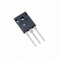
... D 1.43 W/° − °C J stg +150 Symbol Max Unit R 0.7 °C/W θ °C/W θJA MJW21193 MJW21193G MJW21194 MJW21194G 1 http://onsemi.com 16 AMPERES COMPLEMENTARY SILICON POWER TRANSISTORS 250 VOLTS, 200 WATTS TO−247 CASE 340L STYLE MARKING DIAGRAM MJW2119x AYWWG 1 BASE 3 EMITTER 2 COLLECTOR Assembly Location ...

Page 2

ELECTRICAL CHARACTERISTICS Characteristic OFF CHARACTERISTICS Collector−Emitter Sustaining Voltage (I = 100 mAdc Collector Cutoff Current (V = 200 Vdc Emitter Cutoff Current ( Vdc ...

Page 3

PNP MJW21193 1000 T = 100°C J 25°C 100 0.1 1.0 I COLLECTOR CURRENT (AMPS) C Figure 3. DC Current Gain, V PNP MJW21193 1000 T = 100°C J 25°C 100 - 25°C V ...

Page 4

PNP MJW21193 3 25°C 2 2.0 1.5 1.0 V BE(sat) 0.5 V CE(sat) 0 0.1 1 COLLECTOR CURRENT (AMPS) C Figure 9. Typical Saturation Voltages PNP MJW21193 10 ...

Page 5

There are two limitations on the power handling ability of a transistor; average junction temperature and secondary breakdown. Safe operating area curves indicate I limits of the transistor that must be observed for reliable operation; i.e., the transistor must not ...

Page 6

AUDIO PRECISION MODEL ONE PLUS SOURCE TOTAL HARMONIC AMPLIFIER DISTORTION ANALYZER Figure 18. Total Harmonic Distortion Test Circuit http://onsemi.com 6 + Ω DUT 0.5 Ω 0.5 Ω 8.0 Ω DUT -50 V ...

Page 7

... Opportunity/Affirmative Action Employer. This literature is subject to all applicable copyright laws and is not for resale in any manner. PUBLICATION ORDERING INFORMATION LITERATURE FULFILLMENT: Literature Distribution Center for ON Semiconductor P.O. Box 5163, Denver, Colorado 80217 USA Phone: 303−675−2175 or 800−344−3860 Toll Free USA/Canada Fax: 303− ...

Related keywords