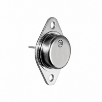
MJ4502G ON Semiconductor, MJ4502G Datasheet - Page 3

MJ4502G
Manufacturer Part Number
MJ4502G
Description
TRANS PWR PNP 30A 100V TO3
Manufacturer
ON Semiconductor
Type
High Powerr
Specifications of MJ4502G
Transistor Type
PNP
Current - Collector (ic) (max)
30A
Voltage - Collector Emitter Breakdown (max)
100V
Vce Saturation (max) @ Ib, Ic
800mV @ 750mA, 7.5A
Dc Current Gain (hfe) (min) @ Ic, Vce
25 @ 7.5A, 2V
Power - Max
200W
Frequency - Transition
2MHz
Mounting Type
Chassis Mount
Package / Case
TO-204, TO-3
Transistor Polarity
NPN
Mounting Style
Through Hole
Collector- Emitter Voltage Vceo Max
90 V
Emitter- Base Voltage Vebo
4 V
Maximum Dc Collector Current
30 A
Power Dissipation
200 W
Maximum Operating Temperature
+ 200 C
Continuous Collector Current
30 A
Dc Collector/base Gain Hfe Min
25
Maximum Operating Frequency
2 MHz
Minimum Operating Temperature
- 65 C
Current, Collector
30 A
Current, Gain
100
Frequency
2 MHz
Package Type
TO-204AA (TO-3)
Polarity
PNP
Primary Type
Si
Resistance, Thermal, Junction To Case
0.875 °C/W
Voltage, Breakdown, Collector To Emitter
100 V
Voltage, Collector To Base
100 V
Voltage, Collector To Emitter
100 V
Voltage, Collector To Emitter, Saturation
0.8 V
Voltage, Emitter To Base
90 V
Number Of Elements
1
Collector-emitter Voltage
90V
Collector-base Voltage
100V
Emitter-base Voltage
4V
Collector Current (dc) (max)
30A
Dc Current Gain (min)
25
Frequency (max)
2MHz
Operating Temp Range
-65C to 200C
Operating Temperature Classification
Military
Mounting
Through Hole
Pin Count
2 +Tab
Lead Free Status / RoHS Status
Lead free / RoHS Compliant
Current - Collector Cutoff (max)
-
Lead Free Status / Rohs Status
Lead free / RoHS Compliant
Other names
MJ4502GOS
100
5.0
2.0
1.0
0.5
0.2
0.1
50
20
10
1.0
3.0
2.0
1.0
0.7
0.5
0.3
0.2
0.1
0.03
Figure 4. Active Region Safe Operating Area
T
J
DATA SHOWN IS OBTAINED FROM PULSE TESTS
AND ADJUSTED TO NULLIFY EFFECT OF I
= 200°C
0.05
2.0 3.0
V
CE
SECONDARY BREAKDOWN LIMITED
BONDING WIRE LIMITED
THERMAL LIMITATIONS @ T
PULSE DUTY CYCLE v 10%
, COLLECTOR‐EMITTER VOLTAGE (VOLTS)
0.1
Figure 2. DC Current Gain
I
0.2 0.3
C
T
, COLLECTOR CURRENT (AMP)
5.0
J
- 55°C
= 175°C
25°C
dc
0.5
10
1.0
C
20
2.0
= 25°C
3.0 5.0
CBO
30
1.0 ms
.
5.0 ms
V
100 ms
50
CE
10
= 2.0 V
http://onsemi.com
100
20
30
3
below which the device will not enter secondary breakdown.
Collector load lines for specific circuits must fall within the
applicable Safe Area to avoid causing a catastrophic failure.
To
power−temperature derating must be observed for both
steady state and pulse power conditions.
The Safe Operating Area Curves indicate I
2.0
1.8
1.6
1.4
1.2
1.0
0.8
0.6
0.4
0.2
0
0.03 0.05
insure
V
V
BE(sat)
V
CE(sat)
T
0.1
BE
operation
J
= 25°C
@ V
@ I
@ I
I
0.2 0.3
C
Figure 3. “On” Voltages
CE
, COLLECTOR CURRENT (AMP)
C
C
/I
/I
B
= 2.0 V
B
= 10
= 10
0.5
below
1.0
2.0
the
3.0 5.0
maximum
C
− V
10
CE
limits
20
T
30
J
,


