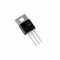
2N6109G ON Semiconductor, 2N6109G Datasheet - Page 3

2N6109G
Manufacturer Part Number
2N6109G
Description
TRANS PNP PWR GP 7A 50V TO220AB
Manufacturer
ON Semiconductor
Type
Powerr
Specifications of 2N6109G
Transistor Type
PNP
Current - Collector (ic) (max)
7A
Voltage - Collector Emitter Breakdown (max)
50V
Vce Saturation (max) @ Ib, Ic
3.5V @ 3A, 7A
Current - Collector Cutoff (max)
1mA
Dc Current Gain (hfe) (min) @ Ic, Vce
30 @ 2.5A, 4V
Power - Max
40W
Frequency - Transition
10MHz
Mounting Type
Through Hole
Package / Case
TO-220-3 (Straight Leads)
Transistor Polarity
PNP
Mounting Style
Through Hole
Collector- Emitter Voltage Vceo Max
50 V
Emitter- Base Voltage Vebo
5 V
Maximum Dc Collector Current
7 A
Power Dissipation
40 W
Maximum Operating Temperature
+ 150 C
Continuous Collector Current
7 A
Dc Collector/base Gain Hfe Min
30
Maximum Operating Frequency
10 MHz
Minimum Operating Temperature
- 65 C
Current, Collector
7 A
Current, Gain
2.3
Frequency
1 MHz
Package Type
TO-220AB
Polarity
PNP
Primary Type
Si
Resistance, Thermal, Junction To Case
3.125 °C/W
Voltage, Breakdown, Collector To Emitter
50 V
Voltage, Collector To Base
60 V
Voltage, Collector To Emitter
50 V
Voltage, Collector To Emitter, Saturation
3.5 V
Voltage, Emitter To Base
5 V
Collector Emitter Voltage V(br)ceo
50V
Transition Frequency Typ Ft
10MHz
Power Dissipation Pd
40W
Dc Collector Current
-7A
Dc Current Gain Hfe
10
Rohs Compliant
Yes
Lead Free Status / RoHS Status
Lead free / RoHS Compliant
Other names
2N6109GOS
ORDERING INFORMATION
0.15
2N6107
2N6107G
2N6109
2N6109G
2N6111
2N6111G
2N6288
2N6288G
2N6292
2N6292G
7.0
5.0
3.0
2.0
1.0
0.7
0.5
0.3
0.2
15
10
0.07
0.05
5.0
3.0
2.0
1.0
0.7
0.5
0.3
0.2
0.1
1.0
0.07
Figure 5. Active-Region Safe Operating Area
0.1
2.0 3.0
V
CE
Device
, COLLECTOR-EMITTER VOLTAGE (VOLTS)
CURRENT LIMIT
SECONDARY
BREAKDOWN LIMIT
THERMAL LIMIT
@ T
0.2
C
t
t
I
s
r
C
Figure 6. Turn-Off Time
= 25°C (SINGLE PULSE)
0.3
, COLLECTOR CURRENT (AMP)
5.0
PNP - 2N6107, 2N6109, 2N6111; NPN - 2N6288, 2N6292
7.0
0.5
10
dc
1.0
20
Device Marking
0.5 ms
30
2N6107
2N6109
2N6288
2N6292
2N6111
2.0
T
V
I
I
C
B1
J
CC
/I
= 25°C
B
= I
= 30 V
= 10
3.0
B2
50 70 100
0.1 ms
5.0 ms
5.0
0.1
ms
7.0
4
a transistor: average junction temperature and second
breakdown. Safe operating area curves indicate I
limits of the transistor that must be observed for reliable
operation; i.e., the transistor must not be subjected to greater
dissipation than the curves indicate.
variable depending on conditions. Second breakdown
pulse limits are valid for duty cycles to 10% provided
T
Figure 4. At high case temperatures, thermal limitations will
reduce the power that can be handled to values less than the
limitations imposed by second breakdown.
J(pk)
300
200
100
There are two limitations on the power handling ability of
The data of Figure 5 is based on T
70
50
30
TO-220AB
TO-220AB
TO-220AB
TO-220AB
TO-220AB
TO-220AB
TO-220AB
TO-220AB
TO-220AB
TO-220AB
(Pb-Free)
(Pb-Free)
(Pb-Free)
(Pb-Free)
(Pb-Free)
Package
0.5
v 150_C. T
1.0
V
J(pk)
R
Figure 7. Capacitance
2.0
, REVERSE VOLTAGE (VOLTS)
may be calculated from the data in
C
3.0
C
ob
ib
5.0
50 Units / Rail
50 Units / Rail
50 Units / Rail
50 Units / Rail
50 Units / Rail
Shipping
10
J(pk)
T
J
= 150_C; T
= 25°C
20
30
C
- V
C
50
CE
is


