NSS12100M3T5G ON Semiconductor, NSS12100M3T5G Datasheet

TRANSISTOR PNP 1A 12V SOT-723

NSS12100M3T5G

Manufacturer Part Number
NSS12100M3T5G
Description
TRANSISTOR PNP 1A 12V SOT-723
Manufacturer
ON Semiconductor
Datasheet

Specifications of NSS12100M3T5G

Transistor Type
PNP
Current - Collector (ic) (max)
1A
Voltage - Collector Emitter Breakdown (max)
12V
Vce Saturation (max) @ Ib, Ic
410mV @ 100mA, 1A
Dc Current Gain (hfe) (min) @ Ic, Vce
120 @ 500mA, 2V
Power - Max
460mW
Mounting Type
Surface Mount
Package / Case
SOT-723
Configuration
Single
Transistor Polarity
PNP
Mounting Style
SMD/SMT
Collector- Emitter Voltage Vceo Max
12 V
Emitter- Base Voltage Vebo
5 V
Continuous Collector Current
- 1 A
Maximum Dc Collector Current
1 A
Power Dissipation
625 mW
Maximum Operating Temperature
+ 150 C
Dc Collector/base Gain Hfe Min
80
Minimum Operating Temperature
- 55 C
Lead Free Status / RoHS Status
Lead free / RoHS Compliant
Current - Collector Cutoff (max)
-
Frequency - Transition
-
Lead Free Status / Rohs Status
Lead free / RoHS Compliant
Other names
NSS12100M3T5G

Available stocks

Company
Part Number
Manufacturer
Quantity
Price
Part Number:
NSS12100M3T5G
Manufacturer:
ON Semiconductor
Quantity:
3 900
Part Number:
NSS12100M3T5G
Manufacturer:
ON
Quantity:
30 000
NSS12100M3T5G
12 V, 1 A, Low V
PNP Transistor
transistors are miniature surface mount devices featuring ultra low
saturation voltage (V
are designed for use in low voltage, high speed switching applications
where affordable efficient energy control is important.
in portable and battery powered products such as cellular and cordless
phones, PDAs, computers, printers, digital cameras and MP3 players.
Other applications are low voltage motor controls in mass storage
products such as disc drives and tape drives. In the automotive
industry they can be used in air bag deployment and in the instrument
cluster. The high current gain allows e
driven directly from PMU's control outputs, and the Linear Gain
(Beta) makes them ideal components in analog amplifiers.
Features
Benefits
Stresses exceeding Maximum Ratings may damage the device. Maximum
Ratings are stress ratings only. Functional operation above the Recommended
Operating Conditions is not implied. Extended exposure to stresses above the
Recommended Operating Conditions may affect device reliability.
MAXIMUM RATINGS
© Semiconductor Components Industries, LLC, 2007
September, 2007 - Rev. 0
Collector‐Emitter Voltage
Collector‐Base Voltage
Emitter‐Base Voltage
Collector Current - Continuous
Collector Current
Electrostatic Discharge
ON Semiconductor's e
Typical application are DC-DC converters and power management
High Specific Current and Power Capability Reduces Required PCB Area
High Continuous Current Capability (1 A)
Low V
Small Size 1.2 mm x 1.2 mm
This is a Pb-Free Device
Reduced Parasitic Losses Increases Battery Life
CE(sat)
Rating
(150 mV Typical @ 500 mA)
- Peak
CE(sat)
(T
A
= 25°C)
) and high current gain capability. These
2
PowerEdge family of low V
Symbol
V
V
V
ESD
I
CEO
CBO
EBO
I
CM
C
CE(sat)
2
PowerEdge devices to be
HBM Class 3B
Max
-5.0
-1.0
-3.0
-12
-12
MM Class C
1
CE(sat)
Unit
Vdc
Vdc
Vdc
Adc
†For information on tape and reel specifications,
NSS12100M3T5G
PNP LOW V
including part orientation and tape sizes, please
refer to our Tape and Reel Packaging Specifications
Brochure, BRD8011/D.
EQUIVALENT R
3
Device
1
12 VOLTS, 1.0 AMPS
ORDERING INFORMATION
VE = Specific Device Code
M
BASE
2
http://onsemi.com
1
= Date Code
CE(sat)
CASE 631AA
SOT-723
STYLE 1
(Pb-Free)
SOT-723
Package
COLLECTOR
Publication Order Number:
DS(on)
EMITTER
TRANSISTOR
3
2
NSS12100M3/D
350 mW
Tape & Reel
MARKING
DIAGRAM
Shipping
8000/
VE M

Related parts for NSS12100M3T5G

NSS12100M3T5G Summary of contents

Page 1

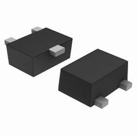
... STYLE Specific Device Code M = Date Code ORDERING INFORMATION Device Package Shipping NSS12100M3T5G SOT-723 8000/ (Pb-Free) Tape & Reel †For information on tape and reel specifications, including part orientation and tape sizes, please refer to our Tape and Reel Packaging Specifications Brochure, BRD8011/D. Publication Order Number: ...

Page 2

... 1.0 MHz) EB Output Capacitance ( 1.0 MHz) CB Noise Figure (I = 0 100 copper traces FR 500 copper traces. 3. Pulsed Condition: Pulse Width = 300 msec, Duty Cycle ≤ 2%. 4. Guaranteed by design but not tested. NSS12100M3T5G 25°C unless otherwise noted -10 mAdc -0.1 mAdc ...

Page 3

... -55°C BE(sat) 0.8 25°C 0.6 150°C 0.4 0.2 0 0.00001 0.0001 0.001 I , COLLECTOR CURRENT (A) C Figure 5. Base Emitter Saturation Voltage vs. Collector Current NSS12100M3T5G 2.0 1 100 150°C 1.6 CE(sat) 1.4 1.2 25°C 1.0 0.8 -55°C 0.6 0.4 0.2 0 ...

Page 4

... C 2.5 2.0 1.5 1.0 0 0.01 0 BASE CURRENT (mA) B Figure 7. Saturation Region @ 255C obo(pF COLLECTOR BASE VOLTAGE (V) CB Figure 9. Output Capacitance NSS12100M3T5G ibo(pF 100 Figure 8. Input Capacitance 10 1 0.1 Power Limit Package Limit 0.01 0 COLLECTOR-EMITTER VOLTAGE (V) CE Figure 10. Safe Operating Area http://onsemi ...

Page 5

... LITERATURE FULFILLMENT:  Literature Distribution Center for ON Semiconductor  P.O. Box 5163, Denver, Colorado 80217 USA  Phone: 303-675-2175 or 800-344-3860 Toll Free USA/Canada  Fax: 303-675-2176 or 800-344-3867 Toll Free USA/Canada  Email: orderlit@onsemi.com NSS12100M3T5G PACKAGE DIMENSIONS SOT-723 CASE 631AA-01 ISSUE C NOTES: 1. DIMENSIONING AND TOLERANCING PER ANSI 2 ...

Related keywords