NSTB60BDW1T1 ON Semiconductor, NSTB60BDW1T1 Datasheet
NSTB60BDW1T1
Specifications of NSTB60BDW1T1
Available stocks


Related parts for NSTB60BDW1T1

NSTB60BDW1T1 Summary of contents
Page 1
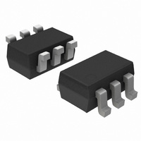
... C/W JL 208 (Note –55 to +150 C stg 1 http://onsemi.com (3) (2) ( (4) (5) ( SOT–363 CASE 419B STYLE 1 MARKING DIAGRAM Specific Device Code d = Date Code ORDERING INFORMATION Device Package Shipping NSTB60BDW1T1 SOT–363 3000/Tape & Reel Publication Order Number: NSTB60BDW1T1/D ...
Page 2
... Collector-Emitter Saturation Voltage ( mA 5.0 mA) (Note Current Gain ( 5.0 mA) (Note Output Voltage ( Output Voltage (off 5 0. Input Resistor (Note 3) Resistor Ratio (Note 3) 3. Pulse Test: Pulse Width < 300 s, Duty Cycle < 2.0% NSTB60BDW1T1 ( unless otherwise noted) A Symbol = (BR)CBO V (BR)CEO = (BR)EBO = CBO = EBO V ...
Page 3
... Typical Electrical Characteristics – PNP Transistor Figure 1. Normalized DC Current Gain Figure 3. Current–Gain – Bandwidth Product Figure 5. Output Admittance NSTB60BDW1T1 Figure 2. “Saturation” and “On” Voltages Figure 4. Capacitances Figure 6. Base Spreading Resistance http://onsemi.com 3 ...
Page 4
... B 0.1 0. COLLECTOR CURRENT (mA) C Figure 7. Maximum Collector Voltage versus Collector Current 4 3.5 3 2.5 2 1 REVERSE BIAS VOLTAGE (V) R Figure 9. Output Capacitance 100 10 1 0.1 0 Figure 11. Input Voltage versus Output Current NSTB60BDW1T1 1000 – 100 100 MHz 0.1 0. Figure 10. Output Current versus Input T = – ...
Page 5
... Thermal Clad, an aluminum core board, the power dissipation can be doubled using the same footprint. NSTB60BDW1T1 interface between the board and the package. With the correct pad geometry, the packages will self align when subjected to a solder reflow process. ...
Page 6
... This profile shows temperature versus time. NSTB60BDW1T1 SOLDER STENCIL GUIDELINES The stencil opening size for the surface mounted package should be the same as the pad size on the printed circuit board, i ...
Page 7
... PACKAGE DIMENSIONS –B– NSTB60BDW1T1 SOT–363 CASE 419B–02 ISSUE http://onsemi.com 7 ...
Page 8
... N. American Technical Support: 800–282–9855 Toll Free USA/Canada NSTB60BDW1T1 JAPAN: ON Semiconductor, Japan Customer Focus Center 4–32–1 Nishi–Gotanda, Shinagawa–ku, Tokyo, Japan 141–0031 Phone: 81–3–5740–2700 Email: r14525@onsemi.com ON Semiconductor Website: http://onsemi.com For additional information, please contact your local Sales Representative. http://onsemi.com 8 NSTB60BDW1T1/D ...