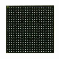
XC4VLX60-11FFG668C Xilinx Inc, XC4VLX60-11FFG668C Datasheet - Page 37

XC4VLX60-11FFG668C
Manufacturer Part Number
XC4VLX60-11FFG668C
Description
FPGA Virtex®-4 Family 59904 Cells 90nm (CMOS) Technology 1.2V 668-Pin FCBGA
Manufacturer
Xilinx Inc
Series
Virtex™-4r
Specifications of XC4VLX60-11FFG668C
Package
668FCBGA
Family Name
Virtex®-4
Device Logic Units
59904
Typical Operating Supply Voltage
1.2 V
Maximum Number Of User I/os
448
Ram Bits
2949120
Number Of Logic Elements/cells
59904
Number Of Labs/clbs
6656
Total Ram Bits
2949120
Number Of I /o
448
Voltage - Supply
1.14 V ~ 1.26 V
Mounting Type
Surface Mount
Operating Temperature
0°C ~ 85°C
Package / Case
668-BBGA, FCBGA
Lead Free Status / RoHS Status
Lead free / RoHS Compliant
For Use With
HW-AFX-FF668-400 - BOARD DEV VIRTEX 4 FF668
Number Of Gates
-
Lead Free Status / RoHS Status
Lead free / RoHS Compliant
Other names
122-1496
Available stocks
Company
Part Number
Manufacturer
Quantity
Price
Company:
Part Number:
XC4VLX60-11FFG668C
Manufacturer:
Xilinx Inc
Quantity:
10 000
Table 43: Configuration Switching Characteristics (Continued)
DS302 (v3.7) September 9, 2009
Product Specification
Notes:
1.
2.
Boundary-Scan Port Timing Specifications
Dynamic Reconfiguration Port (DRP) for DCM
T
T
T
F
F
CLKIN_FREQ_DLL_HF_MS_MAX
T
T
T
T
T
T
T
do not apply to the BUFGMUX_VIRTEX4 primitive that assures glitch-free operation. The other global clock setup and hold times are optional; only
needing to be satisfied if device operation requires simulation matches on a cycle-for-cycle basis when switching between clocks.
DO holds until the next DRP operation.
TAPTCK
TCKTAP
TCKTDO
TCK
TCKB
DMCCK_DADDR
DMCCK_DI
DMCCK_DEN
DMCCK_DWE
DMCKO_DO
DMCKO_DRDY
BCCCK_CE
/T
and T
DMCKC_DI
/T
/T
Symbol
DMCKC_DEN
DMCKC_DWE
/T
BCCKC_CE
DMCKC_DADDR
must be satisfied to assure glitch-free operation of the global clock when switching between clocks. These parameters
TMS and TDI Setup time before TCK
TMS and TDI Hold time after TCK
TCK falling edge to TDO output valid
Maximum configuration TCK clock
frequency
Maximum Boundary-Scan TCK clock
frequency
Maximum frequency for DCLK
DADDR Setup/Hold time
DI Setup/Hold time
DEN Setup/Hold time
DWE Setup/Hold time
CLK to out of DO
CLK to out of DRDY
www.xilinx.com
Description
Virtex-4 FPGA Data Sheet: DC and Switching Characteristics
(2)
0.54
0.00
0.54
0.00
0.58
0.00
0.58
0.00
0.68
-12
500
1.0
2.0
6.0
66
50
0
Speed Grade
0.63
0.00
0.63
0.00
0.58
0.00
0.58
0.00
0.80
-11
450
1.0
2.0
6.0
66
50
0
0.72
0.00
0.72
0.00
0.58
0.00
0.58
0.00
0.92
-10
400
1.0
2.0
6.0
66
50
0
MHz, Max
MHz, Max
MHz, Max
ns, Max
ns, Max
ns, Max
ns, Max
ns, Max
ns, Max
ns, Max
ns, Min
ns, Min
Units
37


