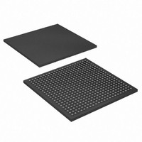
XC3SD3400A-4CSG484C Xilinx Inc, XC3SD3400A-4CSG484C Datasheet - Page 3

XC3SD3400A-4CSG484C
Manufacturer Part Number
XC3SD3400A-4CSG484C
Description
FPGA Spartan®-3A Family 3.4M Gates 53712 Cells 667MHz 90nm Technology 1.2V 484-Pin LCSBGA
Manufacturer
Xilinx Inc
Series
Spartan™-3A DSPr
Datasheets
1.XC3S50A-4VQG100C.pdf
(7 pages)
2.XC3SD3400A-4FGG676C.pdf
(4 pages)
3.XC3SD3400A-4FGG676C.pdf
(101 pages)
Specifications of XC3SD3400A-4CSG484C
Package
484LCSBGA
Family Name
Spartan®-3A
Device Logic Units
53712
Device System Gates
3400000
Maximum Internal Frequency
667 MHz
Typical Operating Supply Voltage
1.2 V
Maximum Number Of User I/os
309
Ram Bits
2322432
Number Of Logic Elements/cells
53712
Number Of Labs/clbs
5968
Total Ram Bits
2322432
Number Of I /o
309
Number Of Gates
3400000
Voltage - Supply
1.14 V ~ 1.26 V
Mounting Type
Surface Mount
Operating Temperature
0°C ~ 85°C
Package / Case
484-FBGA, CSPBGA
Lead Free Status / RoHS Status
Lead free / RoHS Compliant
For Use With
122-1532 - KIT DEVELOPMENT SPARTAN 3ADSP
Lead Free Status / RoHS Status
Lead free / RoHS Compliant
Other names
122-1540
Available stocks
Company
Part Number
Manufacturer
Quantity
Price
Company:
Part Number:
XC3SD3400A-4CSG484C
Manufacturer:
XILINX
Quantity:
177
Company:
Part Number:
XC3SD3400A-4CSG484C
Manufacturer:
XILINX
Quantity:
110
Part Number:
XC3SD3400A-4CSG484C
Manufacturer:
XILINX/赛灵思
Quantity:
20 000
Company:
Part Number:
XC3SD3400A-4CSG484CL
Manufacturer:
XILINX
Quantity:
123
Architectural Overview
The Spartan-3A DSP family architecture consists of five fundamental programmable functional elements:
•
•
•
•
X-Ref Target - Figure 1
DS610 (v3.0) October 4, 2010
Product Specification
XtremeDSP™ DSP48A Slice provides an 18-bit x
18-bit multiplier, 18-bit pre-adder, 48-bit
post-adder/accumulator, and cascade capabilities for
various DSP applications.
Block RAM provides data storage in the form of
18-Kbit dual-port blocks.
Configurable Logic Blocks (CLBs) contain flexible
Look-Up Tables (LUTs) that implement logic plus
storage elements used as flip-flops or latches. CLBs
perform a wide variety of logical functions as well as
store data.
Input/Output Blocks (IOBs) control the flow of data
between the I/O pins and the internal logic of the
device. IOBs support bidirectional data flow plus
3-state operation. Supports a variety of signal
standards, including several high-performance
differential standards. Double Data-Rate (DDR)
registers are included.
Notes:
1.
2.
The XC3SD1800A and XC3SD3400A have two DCMs on both the left and right sides, as well as the two DCMs at the top and
bottom of the devices. The two DCMs on the left and right of the chips are in the middle of the outer Block RAM/DSP48A
columns of the 4 or 5 columns in the selected device, as shown in the diagram above.
A detailed diagram of the DSP48A can be found in UG431: XtremeDSP DSP48A for Spartan-3A DSP FPGAs User Guide.
DCM
CLBs
IOBs
IOBs
DCM
Figure 1: Spartan-3A DSP Family Architecture
Spartan-3A DSP FPGA Family: Introduction and Ordering Information
DCM
www.xilinx.com
•
These elements are organized as shown in
ring of staggered IOBs surrounds a regular array of CLBs.
The XC3SD1800A has four columns of DSP48As, and the
XC3SD3400A has five columns of DSP48As. Each
DSP48A has an associated block RAM. The DCMs are
positioned in the center with two at the top and two at the
bottom of the device and in the two outer columns of the 4 or
5 columns of block RAM and DSP48As.
The Spartan-3A DSP family features a rich network of
routing that interconnect all five functional elements,
transmitting signals among them. Each functional element
has an associated switch matrix that permits multiple
connections to the routing.
IOBs
Digital Clock Manager (DCM) Blocks provide
self-calibrating, fully digital solutions for distributing,
delaying, multiplying, dividing, and phase-shifting clock
signals.
CLB
DS610-1_01_031207
Figure
1. A dual
3


