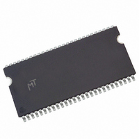
MT48LC8M16A2TG-7E IT:G Micron Technology Inc, MT48LC8M16A2TG-7E IT:G Datasheet - Page 27

MT48LC8M16A2TG-7E IT:G
Manufacturer Part Number
MT48LC8M16A2TG-7E IT:G
Description
DRAM Chip SDRAM 128M-Bit 8Mx16 3.3V 54-Pin TSOP-II Tray
Manufacturer
Micron Technology Inc
Type
SDRAMr
Datasheet
1.MT48LC8M16A2P-75G_TR.pdf
(74 pages)
Specifications of MT48LC8M16A2TG-7E IT:G
Density
128 Mb
Maximum Clock Rate
143 MHz
Package
54TSOP-II
Address Bus Width
14 Bit
Operating Supply Voltage
3.3 V
Maximum Random Access Time
5.4 ns
Operating Temperature
-40 to 85 °C
Format - Memory
RAM
Memory Type
SDRAM
Memory Size
128M (8Mx16)
Speed
143MHz
Interface
Parallel
Voltage - Supply
3 V ~ 3.6 V
Package / Case
54-TSOP II
Organization
8Mx16
Address Bus
14b
Access Time (max)
5.4ns
Operating Supply Voltage (typ)
3.3V
Package Type
TSOP-II
Operating Temp Range
-40C to 85C
Operating Supply Voltage (max)
3.6V
Operating Supply Voltage (min)
3V
Supply Current
165mA
Pin Count
54
Mounting
Surface Mount
Operating Temperature Classification
Industrial
Lead Free Status / RoHS Status
Contains lead / RoHS non-compliant
Lead Free Status / RoHS Status
Not Compliant, Contains lead / RoHS non-compliant
Figure 13:
PDF: 09005aef8091e66d/Source: 09005aef8091e625
128MSDRAM_2.fm - Rev. N 1/09 EN
Consecutive READ Bursts
Notes:
Data from any READ burst may be truncated with a subsequent READ command, and
data from a fixed-length READ burst may be immediately followed by data from a READ
command. In either case, a continuous flow of data can be maintained. The first data
element from the new burst either follows the last element of a completed burst or the
last desired data element of a longer burst that is being truncated. The new READ
command should be issued x cycles before the clock edge at which the last desired data
element is valid, where x = CL - 1.
This is shown in Figure 13 for L = 2 and CL = 3; data element n + 3 is either the last of a
burst of four or the last desired of a longer burst. The 128Mb SDRAM uses a pipelined
architecture and, therefore, does not require the 2n rule associated with a prefetch archi-
tecture. A READ command can be initiated on any clock cycle following a previous READ
command. Full-speed random read accesses can be performed to the same bank, as
shown in Figure 14 on page 28, or each subsequent READ may be performed to a
different bank.
COMMAND
COMMAND
1. Each READ command may be to any bank. DQM is LOW.
ADDRESS
ADDRESS
CLK
CLK
DQ
DQ
T0
T0
BANK,
COL n
BANK,
READ
COL n
READ
CL = 2
T1
T1
NOP
NOP
CL = 3
27
T2
T2
NOP
NOP
D
OUT
n
Micron Technology, Inc., reserves the right to change products or specifications without notice.
T3
T3
NOP
NOP
D
n + 1
D
n
OUT
OUT
TRANSITIONING DATA
T4
T4
BANK,
BANK,
READ
COL b
READ
COL b
X = 1 cycle
n + 1
n + 2
D
D
OUT
OUT
128Mb: x4, x8, x16 SDRAM
X = 2 cycles
T5
T5
NOP
NOP
n + 2
D
n + 3
D
OUT
OUT
©1999 Micron Technology, Inc. All rights reserved.
T6
T6
NOP
NOP
n + 3
D
D
OUT
OUT
b
DON’T CARE
Operations
T7
NOP
D
OUT
b


