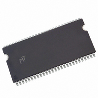
MT48LC16M16A2P-75 L:D TR Micron Technology Inc, MT48LC16M16A2P-75 L:D TR Datasheet - Page 56

MT48LC16M16A2P-75 L:D TR
Manufacturer Part Number
MT48LC16M16A2P-75 L:D TR
Description
DRAM Chip SDRAM 256M-Bit 16Mx16 3.3V 54-Pin TSOP-II T/R
Manufacturer
Micron Technology Inc
Type
SDRAMr
Specifications of MT48LC16M16A2P-75 L:D TR
Package
54TSOP-II
Density
256 Mb
Address Bus Width
15 Bit
Operating Supply Voltage
3.3 V
Maximum Clock Rate
133 MHz
Maximum Random Access Time
6|5.4 ns
Operating Temperature
0 to 70 °C
Format - Memory
RAM
Memory Type
SDRAM
Memory Size
256M (16Mx16)
Speed
133MHz
Interface
Parallel
Voltage - Supply
3 V ~ 3.6 V
Package / Case
54-TSOP II
Lead Free Status / RoHS Status
Lead free / RoHS Compliant
Other names
557-1191-2
- Current page: 56 of 92
- Download datasheet (3Mb)
Figure 24: READ-to-WRITE With Extra Clock Cycle
Figure 25: READ-to-PRECHARGE
PDF: 09005aef8091e6d1
256Mb_sdr.pdf - Rev. N 1/10 EN
Note:
Note:
Command
Command
Command
Address
Address
Address
1. CL = 3. The READ command can be issued to any bank, and the WRITE command can be
1. DQM is LOW.
DQM
CLK
to any bank.
CLK
CLK
DQ
DQ
DQ
Bank a,
Bank a,
Bank,
T0
T0
Col n
T0
READ
Col n
READ
READ
Col
CL = 2
CL = 3
T1
T1
T1
NOP
NOP
NOP
56
T2
T2
T2
NOP
NOP
NOP
D
OUT
Transitioning data
T3
T3
T3
Micron Technology, Inc. reserves the right to change products or specifications without notice.
NOP
NOP
NOP
D
D
D
t HZ
OUT
OUT
OUT
PRECHARGE
PRECHARGE
(a or all)
(a or all)
T4
T4
T4
Bank
Bank
NOP
X = 1 cycle
D
D
Transitioning data
256Mb: x4, x8, x16 SDRAM
OUT
OUT
X = 2 cycles
T5
T5
T5
Don’t Care
Bank,
WRITE
Col b
NOP
NOP
D
D
D
OUT
OUT
IN
t DS
t RP
t RP
© 1999 Micron Technology, Inc. All rights reserved.
T6
T6
READ Operation
NOP
NOP
D
OUT
Don’t Care
ACTIVE
Bank a,
ACTIVE
Bank a,
T7
T7
Row
Row
Related parts for MT48LC16M16A2P-75 L:D TR
Image
Part Number
Description
Manufacturer
Datasheet
Request
R

Part Number:
Description:
DRAM Chip SDRAM 256M-Bit 16Mx16 3.3V 54-Pin TSOP-II Tray
Manufacturer:
Micron Technology Inc
Datasheet:

Part Number:
Description:
DRAM Chip SDRAM 256M-Bit 16Mx16 3.3V 54-Pin TSOP-II Tray
Manufacturer:
Micron Technology Inc
Datasheet:

Part Number:
Description:
IC, SDRAM, 256MBIT, 133MHZ, TSOP-54
Manufacturer:
Micron Technology Inc
Datasheet:

Part Number:
Description:
SDRAM 256MB, SMD, 48LC16, TSOP54
Manufacturer:
Micron Technology Inc
Datasheet:

Part Number:
Description:
Manufacturer:
Micron Technology Inc
Datasheet:

Part Number:
Description:
Manufacturer:
Micron Technology Inc
Datasheet:

Part Number:
Description:
Manufacturer:
Micron Technology Inc
Datasheet:

Part Number:
Description:
IC SDRAM 256MBIT 167MHZ 54TSOP
Manufacturer:
Micron Technology Inc
Datasheet:

Part Number:
Description:
IC SDRAM 256MBIT 133MHZ 54TSOP
Manufacturer:
Micron Technology Inc
Datasheet:

Part Number:
Description:
IC SDRAM 256MBIT 133MHZ 54TSOP
Manufacturer:
Micron Technology Inc
Datasheet:

Part Number:
Description:
IC SDRAM 256MBIT 133MHZ 54TSOP
Manufacturer:
Micron Technology Inc
Datasheet:

Part Number:
Description:
DRAM Chip SDRAM 256M-Bit 16Mx16 3.3V 54-Pin TSOP-II T/R
Manufacturer:
Micron Technology Inc
Datasheet:

Part Number:
Description:
DRAM Chip SDRAM 256M-Bit 16Mx16 3.3V 54-Pin TSOP-II Tray
Manufacturer:
Micron Technology Inc
Datasheet:

Part Number:
Description:
DRAM Chip SDRAM 256M-Bit 16Mx16 3.3V 54-Pin TSOP-II T/R
Manufacturer:
Micron Technology Inc
Datasheet:

Part Number:
Description:
DRAM Chip SDRAM 256M-Bit 16Mx16 3.3V 54-Pin TSOP-II Tray
Manufacturer:
Micron Technology Inc
Datasheet:


