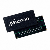
MT46V32M16FN-6:F TR Micron Technology Inc, MT46V32M16FN-6:F TR Datasheet - Page 79

MT46V32M16FN-6:F TR
Manufacturer Part Number
MT46V32M16FN-6:F TR
Description
DRAM Chip DDR SDRAM 512M-Bit 32Mx16 2.5V 60-Pin FBGA T/R
Manufacturer
Micron Technology Inc
Type
DDR SDRAMr
Datasheet
1.MT46V32M16P-5BF_TR.pdf
(91 pages)
Specifications of MT46V32M16FN-6:F TR
Package
60FBGA
Density
512 Mb
Address Bus Width
15 Bit
Operating Supply Voltage
2.5 V
Maximum Clock Rate
333 MHz
Maximum Random Access Time
0.7 ns
Operating Temperature
0 to 70 °C
Format - Memory
RAM
Memory Type
DDR SDRAM
Memory Size
512M (32Mx16)
Speed
6ns
Interface
Parallel
Voltage - Supply
2.3 V ~ 2.7 V
Package / Case
60-FBGA
Lead Free Status / RoHS Status
Contains lead / RoHS non-compliant
- Current page: 79 of 91
- Download datasheet (4Mb)
Figure 44:
PDF: 09005aef80a1d9d4/Source: 09005aef82a95a3a
DDR_x4x8x16_Core2.fm - 512Mb DDR: Rev. N; Core DDR Rev. B 2/09 EN
Command
t DQSS (NOM)
t DQSS (MIN)
t DQSS (MAX)
Address
DQS
DQS
DQS
CK#
DM
DM
DM
DQ
DQ
DQ
CK
WRITE-to-READ – Odd Number of Data, Interrupting
Notes:
Bank a,
WRITE
Col b
T0
t DQSS
t DQSS
t DQSS
1. DI b = data-in for column b; DO n = data-out for column n.
2. An interrupted burst of 4 is shown; one data element is written.
3.
4. A10 is LOW with the WRITE command (auto precharge is disabled).
5. DQS is required at T1n, T2, and T2n (nominal case) to register DM.
6. If the burst of 8 is used, DM and DQS are required at T3–T3n because the READ command
t
the last two data elements).
will not mask these data elements.
DI
b
WTR is referenced from the first positive CK edge after the last desired data-in pair (not
NOP
DI
T1
b
DI
b
T1n
NOP
T2
t WTR
T2n
79
Bank a,
READ
Col n
T3
T3n
Micron Technology, Inc., reserves the right to change products or specifications without notice.
CL = 2
CL = 2
CL = 2
NOP
T4
512Mb: x4, x8, x16 DDR SDRAM
Transitioning Data
T5
NOP
©2000 Micron Technology, Inc. All rights reserved.
DO
DO
DO
n
n
n
T5n
T6
NOP
Operations
Don’t Care
T6n
Related parts for MT46V32M16FN-6:F TR
Image
Part Number
Description
Manufacturer
Datasheet
Request
R

Part Number:
Description:
IC SDRAM 64MBIT 133MHZ 54TSOP
Manufacturer:
Micron Technology Inc
Datasheet:

Part Number:
Description:
IC SDRAM 64MBIT 5.5NS 86TSOP
Manufacturer:
Micron Technology Inc
Datasheet:

Part Number:
Description:
IC SDRAM 64MBIT 200MHZ 86TSOP
Manufacturer:
Micron Technology Inc
Datasheet:

Part Number:
Description:
IC SDRAM 64MBIT 133MHZ 54TSOP
Manufacturer:
Micron Technology Inc
Datasheet:

Part Number:
Description:
IC SDRAM 128MBIT 133MHZ 54TSOP
Manufacturer:
Micron Technology Inc
Datasheet:

Part Number:
Description:
IC SDRAM 256MBIT 133MHZ 90VFBGA
Manufacturer:
Micron Technology Inc
Datasheet:

Part Number:
Description:
IC SDRAM 128MBIT 133MHZ 54TSOP
Manufacturer:
Micron Technology Inc
Datasheet:

Part Number:
Description:
IC SDRAM 256MBIT 133MHZ 54TSOP
Manufacturer:
Micron Technology Inc
Datasheet:

Part Number:
Description:
IC DDR SDRAM 512MBIT 6NS 66TSOP
Manufacturer:
Micron Technology Inc
Datasheet:

Part Number:
Description:
IC SDRAM 128MBIT 167MHZ 86TSOP
Manufacturer:
Micron Technology Inc
Datasheet:

Part Number:
Description:
IC SDRAM 128MBIT 143MHZ 86TSOP
Manufacturer:
Micron Technology Inc
Datasheet:

Part Number:
Description:
SDRAM 256M-BIT 1.8V 54-PIN VFBGA
Manufacturer:
Micron Technology Inc
Datasheet:

Part Number:
Description:
IC SDRAM 128MBIT 143MHZ 86TSOP
Manufacturer:
Micron Technology Inc
Datasheet:

Part Number:
Description:
IC SDRAM 128MBIT 125MHZ 54VFBGA
Manufacturer:
Micron Technology Inc
Datasheet:

Part Number:
Description:
IC SDRAM 128MBIT 125MHZ 54VFBGA
Manufacturer:
Micron Technology Inc
Datasheet:


