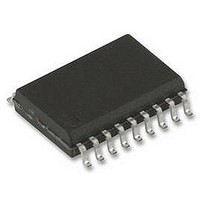
74HCT574D NXP Semiconductors, 74HCT574D Datasheet - Page 8

74HCT574D
Manufacturer Part Number
74HCT574D
Description
Flip Flop D-Type Bus Interface Pos-Edge 3-ST 1-Element 20-Pin SO Bulk
Manufacturer
NXP Semiconductors
Specifications of 74HCT574D
Package
20SO
Logic Function
D-Type Bus Interface
Logic Family
HCT
Number Of Element Outputs
8
Output Signal Type
Single-Ended
Output Type
3-State
Number Of Output Enables Per Element
1
Typical Operating Supply Voltage
5 V
Operating Temperature
-40 to 125 °C
Flip-flop Type
D
Propagation Delay
18ns
Frequency
123MHz
Output Current
6mA
Supply Voltage Range
4.5V To 5.5V
Logic Case Style
SOIC
No. Of Pins
20
Operating
RoHS Compliant
Trigger Type
Positive Edge
Ic Output Type
Tri State Non Inverted
Rohs Compliant
Yes
Lead Free Status / RoHS Status
Available stocks
Company
Part Number
Manufacturer
Quantity
Price
Part Number:
74HCT574D
Manufacturer:
NXP/恩智浦
Quantity:
20 000
NXP Semiconductors
Table 7.
Voltages are referenced to GND (ground = 0 V); C
[1]
[2]
[3]
[4]
[5]
74HC_HCT574
Product data sheet
Symbol Parameter
C
For type 74HCT574
t
t
t
t
t
t
t
f
C
pd
en
dis
t
W
su
h
max
PD
PD
t
t
t
t
C
P
f
f
C
V
N = number of inputs switching;
(C
pd
en
dis
t
i
o
D
CC
PD
= input frequency in MHz;
L
is the same as t
= output frequency in MHz;
is the same as t
is the same as t
= output load capacitance in pF;
= C
is the same as t
L
is used to determine the dynamic power dissipation (P
= supply voltage in V;
V
power
dissipation
capacitance
propagation
delay
enable time
disable time OE to Qn; see
transition
time
pulse width
set-up time
hold time
maximum
frequency
power
dissipation
capacitance
PD
Dynamic characteristics
CC
V
2
f
CC
o
2
) = sum of outputs.
f
THL
PLH
PZH
PLZ
i
N + (C
and t
Conditions
C
V
CP to Qn; see
OE to Qn; see
Qn; see
CP HIGH or LOW;
see
Dn to CP; see
Dn to CP; see
CP; see
C
V
and t
and t
and t
I
I
L
L
V
V
V
V
V
V
V
V
V
V
= GND to V
= GND to V
= 50 pF; f = 1 MHz;
= 50 pF; f = 1 MHz;
TLH
CC
CC
CC
CC
CC
CC
CC
CC
CC
CC
Figure 8
PHL
PZL
PHZ
.
= 4.5 V
= 5 V; C
= 4.5 V
= 4.5 V
= 4.5 V
= 4.5 V
= 4.5 V
= 4.5 V
= 4.5 V
= 5 V; C
L
.
.
.
Figure 7
Figure 7
V
CC
2
…continued
CC
CC
Figure 8
Figure 8
Figure 7
Figure 9
Figure 9
L
L
f
= 15 pF
= 15 pF
o
All information provided in this document is subject to legal disclaimers.
) where:
Rev. 3 — 15 December 2010
L
= 50 pF unless otherwise specified; for test circuit see
[5]
[1]
[2]
[3]
[4]
[5]
D
Min
in W).
16
12
30
5
-
-
-
-
-
-
-
-
Octal D-type flip-flop; positive edge-trigger; 3-state
25 C
Typ
22
18
15
19
16
1
69
76
25
5
7
3
Max
33
33
28
12
-
-
-
-
-
-
-
-
74HC574; 74HCT574
40 C to +85 C 40 C to +125 C Unit
Min
20
15
24
5
-
-
-
-
-
-
-
-
Max
41
41
35
15
-
-
-
-
-
-
-
-
Min
24
18
20
5
-
-
-
-
-
-
-
-
© NXP B.V. 2010. All rights reserved.
Figure
Max
50
50
42
18
-
-
-
-
-
-
-
-
10.
8 of 19
pF
ns
ns
ns
ns
ns
ns
ns
ns
MHz
MHz
pF


