74HC165N NXP Semiconductors, 74HC165N Datasheet - Page 4
74HC165N
Manufacturer Part Number
74HC165N
Description
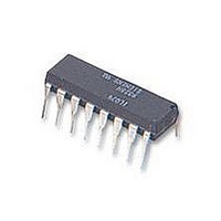
Shift Register Single 8-Bit Serial/Parallel to Serial 16-Pin PDIP Bulk
Manufacturer
NXP Semiconductors
Datasheet
1.74HCT165N652.pdf
(22 pages)
Specifications of 74HC165N
Package
16PDIP
Logic Function
Shift Register
Logic Family
HC
Operation Mode
Serial/Parallel to Serial
Direction Type
Uni-Directional
Number Of Element Inputs
9
Number Of Elements Per Chip
1
Typical Operating Supply Voltage
5 V
Operating Temperature
-40 to 125 °C
Shift Register Function
Parallel To Serial
No. Of Elements
1
Ic Output Type
Standard
Logic Case Style
DIP
No. Of Pins
16
Supply Voltage Range
2V To 6V
Logic Type
Shift Register
Lead Free Status / RoHS Status
Lead free / RoHS Compliant
Available stocks
Company
Part Number
Manufacturer
Quantity
Price
Company:

Part Number:
74HC165N
Manufacturer:
NXP Semiconductors
Quantity:
1 867
Company:
Part Number:
74HC165N
Manufacturer:
PHILIPS
Quantity:
2 149
Company:
Part Number:
74HC165N
Manufacturer:
NXPSemicondu
Quantity:
1 250
Part Number:
74HC165N TI
Manufacturer:
TI/德州仪器
Quantity:
20 000


NXP Semiconductors
Table 2.
7. Functional description
Table 3.
[1]
74HC_HCT165_3
Product data sheet
Symbol
PL
CP
Q7
GND
Q7
DS
D0 to D7
CE
V
Operating modes
parallel load
serial shift
hold “do nothing”
CC
H = HIGH voltage level;
h = HIGH voltage level one set-up time prior to the LOW-to-HIGH clock transition;
L = LOW voltage level;
l = LOW voltage level one set-up time prior to the LOW-to-HIGH clock transition;
q = state of the referenced output one set-up time prior to the LOW-to-HIGH clock transition;
X = don’t care;
= LOW-to-HIGH clock transition.
Pin description
Function table
Pin
1
2
7
8
9
10
11, 12, 13, 14, 3, 4, 5, 6
15
16
6.2 Pin description
Inputs
PL
L
L
H
H
H
H
H
H
[1]
CE
X
X
L
L
H
X
CP
X
X
L
L
X
H
Description
asynchronous parallel load input (active LOW)
clock input (LOW-to-HIGH edge-triggered)
complementary output from the last stage
ground (0 V)
serial output from the last stage
serial data input
parallel data inputs (also referred to as Dn)
clock enable input (active LOW)
positive supply voltage
Rev. 03 — 14 March 2008
DS
X
X
l
h
l
h
X
X
D0 to D7 Q0
L
H
X
X
X
X
X
X
74HC165; 74HCT165
8-bit parallel-in/serial out shift register
Qn registers
L
H
L
H
L
H
q0
q0
Q1 to Q6 Q7
L to L
H to H
q0 to q5
q0 to q5
q0 to q5
q0 to q5
q1 to q6
q1 to q6
Outputs
L
H
q6
q6
q6
q6
q7
q7
© NXP B.V. 2008. All rights reserved.
Q7
H
L
q6
q6
q6
q6
q7
q7
4 of 22