BC847BDW1T1G ON Semiconductor, BC847BDW1T1G Datasheet
BC847BDW1T1G
Specifications of BC847BDW1T1G
Available stocks


Related parts for BC847BDW1T1G


BC847BDW1T1G Summary of contents
Page 1
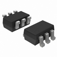
... BC846BDW1T1G, BC847BDW1T1G, BC848CDW1T1G Dual General Purpose Transistors NPN Duals These transistors are designed for general purpose amplifier applications. They are housed in the SOT−363/SC−88 which is designed for low power surface mount applications. Features • These Devices are Pb−Free, Halogen Free/BFR Free and are RoHS ...
Page 2
ELECTRICAL CHARACTERISTICS (T Characteristic OFF CHARACTERISTICS Collector −Emitter Breakdown Voltage ( mA) C Collector −Emitter Breakdown Voltage ( mA Collector −Base Breakdown Voltage ( mA) C Emitter−Base Breakdown Voltage ...
Page 3
TYPICAL CHARACTERISTICS − BC846BDW1T1G 600 500 150°C 400 25°C 300 200 −55°C 100 0 0.001 0. COLLECTOR CURRENT (A) C Figure 1. DC Current Gain 0.20 0.15 0.10 25°C ...
Page 4
TYPICAL CHARACTERISTICS − BC846BDW1T1G 1. 1.10 1.00 0.90 −55°C 0.80 25°C 0.70 0.60 150°C 0.50 0.40 0.30 0.20 0.0001 0.001 I , COLLECTOR CURRENT (A) C Figure BE(on ...
Page 5
... TYPICAL CHARACTERISTICS − BC847BDW1T1G 600 150°C 500 400 25°C 300 −55°C 200 100 0 0.0001 0.001 0. COLLECTOR CURRENT (A) C Figure 12. DC Current Gain 0.20 0.15 0.10 25°C 150°C 0.05 −55°C 0.00 0.0001 0.001 I , COLLECTOR CURRENT (A) C Figure 14. V ...
Page 6
... TYPICAL CHARACTERISTICS − BC847BDW1T1G 1. 1.10 1.00 0.90 −55°C 0.80 0.70 25°C 0.60 0.50 150°C 0.40 0.30 0.20 0.0001 0.001 I , COLLECTOR CURRENT (A) C Figure 18 BE(on 25° 0 REVERSE VOLTAGE (V) R Figure 20. Capacitances V −0.2 CE −0.6 −1 −1.4 −1.8 −2.2 −2.6 −3 0.1 Figure 22. Base− ...
Page 7
TYPICAL CHARACTERISTICS − BC848CDW1T1G 1000 150°C 900 800 700 600 25°C 500 400 −55°C 300 200 100 0 0.0001 0.001 0. COLLECTOR CURRENT (A) C Figure 23. DC Current Gain ...
Page 8
TYPICAL CHARACTERISTICS − BC848CDW1T1G 1 0.9 −55°C 0.8 25°C 0.7 0.6 0.5 0.4 150°C 0.3 0.2 0.1 0.0 0.0001 0.001 0. COLLECTOR CURRENT (A) C Figure 29 BE(on ...
Page 9
... V , COLLECTOR-EMITTER VOLTAGE (V) CE Figure 35. Active Region Safe Operating Area ORDERING INFORMATION Device BC846BDW1T1G BC847BDW1T1G BC847BDW1T3G BC847CDW1T1G BC848CDW1T1G †For information on tape and reel specifications, including part orientation and tape sizes, please refer to our Tape and Reel Packaging Specifications Brochure, BRD8011/D. P (pk) DUTY CYCLE ...
Page 10
... Pb−Free strategy and soldering details, please download the ON Semiconductor Soldering and Mounting Techniques Reference Manual, SOLDERRM/D. ON Semiconductor and are registered trademarks of Semiconductor Components Industries, LLC (SCILLC). SCILLC reserves the right to make changes without further notice to any products herein ...