MAT01GHZ Analog Devices Inc, MAT01GHZ Datasheet
MAT01GHZ
Specifications of MAT01GHZ


Related parts for MAT01GHZ


MAT01GHZ Summary of contents
Page 1
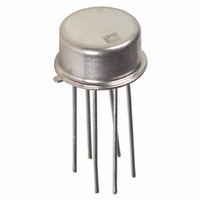
PRODUCT DESCRIPTION The MAT01 is a monolithic dual NPN transistor. An exclusive Silicon Nitride “Triple-Passivation” process provides excellent stability of critical parameters over both temperature and time. Matching characteristics include offset voltage of 40 µV, tem- perature drift of ...
Page 2
MAT01–SPECIFICATIONS ELECTRICAL CHARACTERISTICS Parameter Symbol Breakdown Voltage BV CEO Offset Voltage V OS Offset Voltage Stability First Month V /Time OS Long Term Offset Current I OS Bias Current I B Current Gain h FE ∆h Current Gain Match FE ...
Page 3
TYPICAL ELECTRICAL CHARACTERISTICS Parameter Symbol Average Offset Voltage Drift TCV Average Offset Current Drift TCI Collector-Emitter-Leakage Current I CES Collector-Base-Leakage Current I CBO Gain Bandwidth Product f T ∆V Offset Voltage Stability NOTES 1 Exclude first hour of operation to ...
Page 4
MAT01 1 ABSOLUTE MAXIMUM RATINGS Collector-Base Voltage (BV ) CBO MAT01AH ...
Page 5
Typical Performance Characteristics–MAT01 ...
Page 6
MAT01 MAT01 TEST CIRCUITS ...
Page 7
APPLICATION NOTES Application of reverse bias voltages to the emitter-base junctions in excess of ratings (5 V) may result in degradation matching characteristics. Circuit designs should be checked FE to ensure that reverse bias voltages above 5 ...
Page 8
MAT01 0.040 (1.02) MAX Revision History Location Data Sheet changed from REV REV. B. Edits to FEATURES . . . . . . . . . . . . . . . . . . . . . ...