NST3904DP6T5G ON Semiconductor, NST3904DP6T5G Datasheet - Page 2
NST3904DP6T5G
Manufacturer Part Number
NST3904DP6T5G
Description
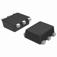
TRANSISTOR NPN DUAL 40V SOT-963
Manufacturer
ON Semiconductor
Datasheet
1.NST3904DP6T5G.pdf
(4 pages)
Specifications of NST3904DP6T5G
Transistor Type
2 NPN (Dual)
Current - Collector (ic) (max)
200mA
Voltage - Collector Emitter Breakdown (max)
40V
Vce Saturation (max) @ Ib, Ic
300mV @ 5mA, 50mA
Dc Current Gain (hfe) (min) @ Ic, Vce
100 @ 10mA, 1V
Power - Max
350mW
Frequency - Transition
200MHz
Mounting Type
Surface Mount
Package / Case
SOT-963
Configuration
Dual
Transistor Polarity
NPN/PNP
Mounting Style
SMD/SMT
Collector- Emitter Voltage Vceo Max
40 V
Emitter- Base Voltage Vebo
6 V
Maximum Dc Collector Current
0.2 A
Power Dissipation
420 mW
Maximum Operating Frequency
200 MHz
Maximum Operating Temperature
+ 150 C
Minimum Operating Temperature
- 55 C
Lead Free Status / RoHS Status
Lead free / RoHS Compliant
Current - Collector Cutoff (max)
-
Lead Free Status / Rohs Status
Lead free / RoHS Compliant
Other names
NST3904DP6T5G
NST3904DP6T5GOSTR
NST3904DP6T5GOSTR
Available stocks
Company
Part Number
Manufacturer
Quantity
Price
Company:

Part Number:
NST3904DP6T5G
Manufacturer:
ON Semiconductor
Quantity:
28 260
Company:
Part Number:
NST3904DP6T5G
Manufacturer:
ON
Quantity:
30 000


4. Pulse Test: Pulse Width ≤ 300 ms; Duty Cycle ≤ 2.0%.
ELECTRICAL CHARACTERISTICS
OFF CHARACTERISTICS
ON CHARACTERISTICS (Note 4)
SMALL−SIGNAL CHARACTERISTICS
SWITCHING CHARACTERISTICS
Collector −Emitter Breakdown Voltage (Note 4) (I
Collector −Base Breakdown Voltage (I
Emitter −Base Breakdown Voltage (I
Collector Cutoff Current (V
DC Current Gain
Collector −Emitter Saturation Voltage
Base −Emitter Saturation Voltage
Current −Gain − Bandwidth Product (I
Output Capacitance (V
Input Capacitance (V
Noise Figure (V
Delay Time
Rise Time
Storage Time
Fall Time
(I
(I
(I
(I
(I
(I
(I
(I
(I
0.28
0.23
0.18
0.13
0.08
0.03
C
C
C
C
C
C
C
C
C
= 0.1 mAdc, V
= 1.0 mAdc, V
= 10 mAdc, V
= 50 mAdc, V
= 100 mAdc, V
= 10 mAdc, I
= 50 mAdc, I
= 10 mAdc, I
= 50 mAdc, I
Figure 1. Collector Emitter Saturation Voltage vs.
0.0001
I
C
/I
B
CE
= 10
= 5.0 Vdc, I
B
B
B
B
CE
CE
I
CE
CE
EB
0.001
= 1.0 mAdc)
= 5.0 mAdc)
= 1.0 mAdc)
= 5.0 mAdc)
C
CE
, COLLECTOR CURRENT (A)
CB
= 1.0 Vdc)
= 1.0 Vdc)
= 1.0 Vdc)
= 1.0 Vdc)
= 0.5 Vdc, I
= 1.0 Vdc)
Collector Current
= 5.0 Vdc, I
CE
= 30 Vdc, V
C
= 100 mAdc, R
Characteristic
(V
(I
(V
(I
C
C
B1
E
0.01
CC
CC
E
C
= 0, f = 1.0 MHz)
= 10 mAdc, I
C
= 10 mAdc, I
V
= I
= 0, f = 1.0 MHz)
= 10 mAdc, V
= 10 mAdc, I
= 3.0 Vdc, V
= 3.0 Vdc, I
CE(sat)
25°C
B2
EB
(T
A
= 1.0 mAdc)
= 3.0 Vdc)
= 25°C unless otherwise noted)
S
= 150°C
= 1.0 k W, f = 1.0 kHz)
C
C
B1
= 1.0 mAdc, I
C
0.1
E
= 0)
BE
CE
= 1.0 mAdc)
= 10 mAdc)
= 0)
−55°C
= − 0.5 Vdc)
= 20 Vdc, f = 100 MHz)
http://onsemi.com
B
= 0)
1
2
350
300
250
200
150
100
400
50
0
0.0001
Figure 2. DC Current Gain vs. Collector Current
150°C (5.0 V)
150°C (1.0 V)
−55°C (5.0 V)
−55°C (1.0 V)
25°C (5.0 V)
25°C (1.0 V)
V
V
V
Symbol
V
V
(BR)CEO
(BR)CBO
(BR)EBO
0.001
I
CE(sat)
BE(sat)
C
C
h
CEX
I
NF
C
f
obo
t
t
FE
t
t
ibo
T
d
s
r
f
, COLLECTOR CURRENT (A)
0.01
0.65
Min
100
200
6.0
40
60
40
70
60
30
−
−
−
−
−
−
−
−
−
−
−
Max
0.85
0.95
300
275
0.2
0.3
4.0
8.0
5.0
50
35
35
50
0.1
−
−
−
−
−
−
−
−
nAdc
MHz
Unit
Vdc
Vdc
Vdc
Vdc
Vdc
dB
pF
pF
ns
ns
−
1
Related parts for NST3904DP6T5G
Image
Part Number
Description
Manufacturer
Datasheet
Request
R

Part Number:
Description:
ON Semiconductor [VOLTAGE REGULATOR]
Manufacturer:
ON Semiconductor
Datasheet:
Part Number:
Description:
357-036-542-201 CARDEDGE 36POS DL .156 BLK LOPRO
Manufacturer:
ON Semiconductor
Datasheet:
Part Number:
Description:
357-036-542-201 CARDEDGE 36POS DL .156 BLK LOPRO
Manufacturer:
ON Semiconductor
Datasheet:
Part Number:
Description:
357-036-542-201 CARDEDGE 36POS DL .156 BLK LOPRO
Manufacturer:
ON Semiconductor
Datasheet:
Part Number:
Description:
357-036-542-201 CARDEDGE 36POS DL .156 BLK LOPRO
Manufacturer:
ON Semiconductor
Datasheet:
Part Number:
Description:
357-036-542-201 CARDEDGE 36POS DL .156 BLK LOPRO
Manufacturer:
ON Semiconductor
Datasheet:
Part Number:
Description:
357-036-542-201 CARDEDGE 36POS DL .156 BLK LOPRO
Manufacturer:
ON Semiconductor
Datasheet:
Part Number:
Description:
357-036-542-201 CARDEDGE 36POS DL .156 BLK LOPRO
Manufacturer:
ON Semiconductor
Datasheet:
Part Number:
Description:
357-036-542-201 CARDEDGE 36POS DL .156 BLK LOPRO
Manufacturer:
ON Semiconductor
Datasheet:
Part Number:
Description:
357-036-542-201 CARDEDGE 36POS DL .156 BLK LOPRO
Manufacturer:
ON Semiconductor
Datasheet:
Part Number:
Description:
357-036-542-201 CARDEDGE 36POS DL .156 BLK LOPRO
Manufacturer:
ON Semiconductor
Datasheet:
Part Number:
Description:
Manufacturer:
ON Semiconductor
Datasheet:
Part Number:
Description:
Manufacturer:
ON Semiconductor
Datasheet:
Part Number:
Description:
Manufacturer:
ON Semiconductor
Datasheet: