MCR12DSMT4 ON Semiconductor, MCR12DSMT4 Datasheet

THYRISTOR SCR 12A 600V DPAK

MCR12DSMT4

Manufacturer Part Number
MCR12DSMT4
Description
THYRISTOR SCR 12A 600V DPAK
Manufacturer
ON Semiconductor
Datasheet

Specifications of MCR12DSMT4

Scr Type
Sensitive Gate
Voltage - Off State
600V
Voltage - Gate Trigger (vgt) (max)
1V
Voltage - On State (vtm) (max)
1.9V
Current - On State (it (av)) (max)
7.6A
Current - On State (it (rms)) (max)
12A
Current - Gate Trigger (igt) (max)
200µA
Current - Hold (ih) (max)
6mA
Current - Off State (max)
10µA
Current - Non Rep. Surge 50, 60hz (itsm)
100A @ 60Hz
Operating Temperature
-40°C ~ 110°C
Mounting Type
Surface Mount
Package / Case
DPak, TO-252 (2 leads+tab), SC-63
Current - On State (it (rms) (max)
12A
Lead Free Status / RoHS Status
Contains lead / RoHS non-compliant
Other names
MCR12DSMT4OSCT

Available stocks

Company
Part Number
Manufacturer
Quantity
Price
Part Number:
MCR12DSMT4G
Manufacturer:
ON
Quantity:
2 500
Part Number:
MCR12DSMT4G
Manufacturer:
ON
Quantity:
12 500
Part Number:
MCR12DSMT4G
Manufacturer:
ON/安森美
Quantity:
20 000
MCR12DSM, MCR12DSN
Sensitive Gate Silicon
Controlled Rectifiers
Reverse Blocking Thyristors
applications such as motor control; process control; temperature, light
and speed control.
Features
Stresses exceeding Maximum Ratings may damage the device. Maximum
Ratings are stress ratings only. Functional operation above the Recommended
Operating Conditions is not implied. Extended exposure to stresses above the
Recommended Operating Conditions may affect device reliability.
1. V
MAXIMUM RATINGS
© Semiconductor Components Industries, LLC, 2008
November, 2008 − Rev. 5
Peak Repetitive Off−State Voltage (Note 1)
(T
60 Hz)
On−State RMS Current
(180° Conduction Angles; T
Average On−State Current
(180° Conduction Angles; T
Peak Non-Repetitive Surge Current
(1/2 Cycle, Sine Wave 60 Hz, T
Circuit Fusing Consideration (t = 8.3 msec)
Forward Peak Gate Power
(Pulse Width ≤ 10 msec, T
Forward Average Gate Power
(t = 8.3 msec, T
Forward Peak Gate Current
(Pulse Width ≤ 10 msec, T
Operating Junction Temperature Range
Storage Temperature Range
Designed for high volume, low cost, industrial and consumer
Small Size
Passivated Die for Reliability and Uniformity
Low Level Triggering and Holding Characteristics
Epoxy Meets UL 94 V−0 @ 0.125 in
ESD Ratings:
Pb−Free Packages are Available
J
apply for zero or negative gate voltage; however, positive gate voltage shall
not be applied concurrent with negative potential on the anode. Blocking
voltages shall not be tested with a constant current source such that the
voltage ratings of the device are exceeded.
DRM
= −40 to 110°C, Sine Wave, 50 Hz to
and V
RRM
C
Rating
= 75°C)
for all types can be applied on a continuous basis. Ratings
MCR12DSM
MCR12DSN
Human Body Model, 3B u 8000 V
Machine Model, C u 400 V
(T
C
J
C
= 25°C unless otherwise noted)
C
C
= 75°C)
= 75°C)
Preferred Device
= 75°C)
= 75°C)
J
= 110°C)
Symbol
I
P
V
V
T(RMS)
I
I
P
T(AV)
I
T
TSM
G(AV)
DRM,
RRM
I
GM
T
GM
stg
2
J
t
−40 to 110
−40 to 150
Value
600
800
100
7.6
5.0
0.5
2.0
12
41
1
A
Unit
2
°C
°C
W
W
V
A
A
A
A
sec
Preferred devices are recommended choices for future use
and best overall value.
1 2
See detailed ordering and shipping information in the package
dimensions section on page 5 of this data sheet.
1
2
3
3
1
2
3
4
Y
WW
R12DSx
G
ORDERING INFORMATION
4
12 AMPERES RMS
4
600 − 800 VOLTS
A
http://onsemi.com
PIN ASSIGNMENT
CASE 369C
CASE 369D
STYLE 4
STYLE 4
DPAK−3
DPAK
= Year
= Work Week
= Device Code
= Pb−Free Package
SCRs
x= M or N
Publication Order Number:
Cathode
Anode
Anode
Gate
G
DIAGRAMS
MARKING
MCR12DSM/D
K
2DSxG
YWW
R1
2DSxG
YWW
R1

Related parts for MCR12DSMT4

MCR12DSMT4 Summary of contents

Page 1

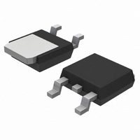
MCR12DSM, MCR12DSN Preferred Device Sensitive Gate Silicon Controlled Rectifiers Reverse Blocking Thyristors Designed for high volume, low cost, industrial and consumer applications such as motor control; process control; temperature, light and speed control. Features • Small Size • Passivated Die ...

Page 2

THERMAL CHARACTERISTICS Characteristic Thermal Resistance,− Junction−to−Case Thermal Resistance − Junction−to−Ambient Thermal Resistance − Junction−to−Ambient (Note 2) Maximum Lead Temperature for Soldering Purposes (Note 3) ELECTRICAL CHARACTERISTICS Characteristics OFF CHARACTERISTICS Peak Repetitive Forward or Reverse Blocking Current (Note ...

Page 3

Voltage Current Characteristic of SCR Symbol Parameter V Peak Repetitive Off State Forward Voltage DRM I Peak Forward Blocking Current DRM V Peak Repetitive Off State Reverse Voltage RRM I Peak Reverse Blocking Current RRM V Peak On State Voltage ...

Page 4

TYPICAL @ T = 25°C J MAXIMUM @ T 10 MAXIMUM @ T = 25°C J 1.0 0.1 0 1.0 2.0 3 INSTANTANEOUS ON-STATE VOLTAGE (VOLTS) T Figure 3. On−State Characteristics 1000 100 GATE OPEN 10 1.0 ...

Page 5

... Figure 11. Exponential Static dv/dt versus Gate−Cathode Resistance and Peak Voltage ORDERING INFORMATION Device MCR12DSMT4 MCR12DSMT4G MCR12DSN−001 MCR12DSN−001G MCR12DSNT4 MCR12DSNT4G †For information on tape and reel specifications, including part orientation and tape sizes, please refer to our Tape and Reel Packaging Specifications Brochure, BRD8011/D ...

Page 6

... 0.13 (0.005) M 5.80 0.228 *For additional information on our Pb−Free strategy and soldering details, please download the ON Semiconductor Soldering and Mounting Techniques Reference Manual, SOLDERRM/D. PACKAGE DIMENSIONS DPAK (SINGLE GAUGE) CASE 369C−01 ISSUE A SEATING −T− PLANE SOLDERING FOOTPRINT* 6.20 3.0 ...

Page 7

... Equal Opportunity/Affirmative Action Employer. This literature is subject to all applicable copyright laws and is not for resale in any manner. PUBLICATION ORDERING INFORMATION LITERATURE FULFILLMENT: Literature Distribution Center for ON Semiconductor P.O. Box 5163, Denver, Colorado 80217 USA Phone: 303−675−2175 or 800−344−3860 Toll Free USA/Canada Fax: 303− ...

Related keywords