MCR22-6RLRA ON Semiconductor, MCR22-6RLRA Datasheet

THYRISTOR SCR 1.5A 400V TO92

MCR22-6RLRA

Manufacturer Part Number
MCR22-6RLRA
Description
THYRISTOR SCR 1.5A 400V TO92
Manufacturer
ON Semiconductor
Datasheet

Specifications of MCR22-6RLRA

Scr Type
Sensitive Gate
Voltage - Off State
400V
Voltage - Gate Trigger (vgt) (max)
800mV
Voltage - On State (vtm) (max)
1.7V
Current - On State (it (rms)) (max)
1.5A
Current - Gate Trigger (igt) (max)
200µA
Current - Hold (ih) (max)
5mA
Current - Off State (max)
10µA
Current - Non Rep. Surge 50, 60hz (itsm)
15A @ 60Hz
Operating Temperature
-40°C ~ 110°C
Mounting Type
Through Hole
Package / Case
TO-92-3 (Standard Body), TO-226
Current - On State (it (rms) (max)
1.5A
Lead Free Status / RoHS Status
Contains lead / RoHS non-compliant
Current - On State (it (av)) (max)
-
Other names
MCR22-6RLRAOSCT

Available stocks

Company
Part Number
Manufacturer
Quantity
Price
Part Number:
MCR22-6RLRAG
Quantity:
20 000
Part Number:
MCR22-6RLRAG
Manufacturer:
ON Semiconductor
Quantity:
190
Part Number:
MCR22-6RLRAG
Manufacturer:
ON/安森美
Quantity:
20 000
Company:
Part Number:
MCR22-6RLRAG
Quantity:
200
MCR22-6, MCR22-8
Sensitive Gate
Silicon Controlled Rectifiers
Reverse Blocking Thyristors
ignition, fuel ignitors, flash circuits, motor controls and low−power
switching applications.
Features
Stresses exceeding Maximum Ratings may damage the device. Maximum
Ratings are stress ratings only. Functional operation above the Recommended
Operating Conditions is not implied. Extended exposure to stresses above the
Recommended Operating Conditions may affect device reliability.
1. V
*For additional information on our Pb−Free strategy and soldering details, please
MAXIMUM RATINGS
THERMAL CHARACTERISTICS
November, 2008 − Rev. 6
download the ON Semiconductor Soldering and Mounting Techniques
Reference Manual, SOLDERRM/D.
Peak Repetitive Off−State Voltage (Note 1)
(R
50 to 60 Hz, R
On−State Current RMS
(180 Conduction Angles, T
Peak Non−repetitive Surge Current,
@T
Circuit Fusing Considerations (t = 8.3 ms)
Forward Peak Gate Power
(Pulse Width
Forward Average Gate Power
(t = 8.3 msec, T
Forward Peak Gate Current
(Pulse Width
Reverse Peak Gate Voltage
(Pulse Width
Operating Junction Temperature Range
@ Rated V
Storage Temperature Range
Thermal Resistance, Junction−to−Case
Thermal Resistance, Junction−to−Ambient
Lead Solder Temperature
(Lead Length q 1/16 from case, 10 S Max)
Designed and tested for repetitive peak operation required for CD
150 A for 2 ms Safe Area
High dv/dt
Very Low Forward “On” Voltage at High Current
Low−Cost TO−226 (TO−92)
Pb−Free Packages are Available*
Semiconductor Components Industries, LLC, 2008
apply for zero or negative gate voltage; however, positive gate voltage shall
not be applied concurrent with negative potential on the anode. Blocking
voltages shall not be tested with a constant current source such that the
voltage ratings of the devices are exceeded.
GK
A
DRM
= 25 C, (1/2 Cycle, Sine Wave, 60 Hz)
= IK, T
and V
RRM
J
= *40 to +110 C, Sine Wave,
RRM
GK
Characteristic
1.0 ms, T
1.0 ms, T
1.0 msec, T
A
and V
= 25 C)
= 1kW)
Rating
for all types can be applied on a continuous basis. Ratings
DRM
A
A
(T
= 25 C)
= 25 C)
J
A
C
= 25 C unless otherwise noted)
= 25 C)
Preferred Device
= 80 C)
MCR22−6
MCR22−8
Symbol
Symbol
I
P
V
T(RMS)
V
V
I
R
R
I
P
G(AV)
FGM
T
DRM,
TSM
RRM
RGM
T
I
T
GM
qJC
qJA
2
stg
J
L
t
−40 to +110
−40 to +150
Value
+260
Max
400
600
160
1.5
0.9
0.5
0.1
0.2
5.0
15
50
1
Unit
Unit
A
C/W
C/W
W
W
V
A
A
A
V
C
C
C
2
s
See detailed ordering and shipping information in the package
dimensions section on page 7 of this data sheet.
Preferred devices are recommended choices for future use
and best overall value.
STRAIGHT LEAD
1 2
BULK PACK
(Note: Microdot may be in either location)
1
2
3
3
MCR22−x = Device Code
A
Y
WW
G
ORDERING INFORMATION
400 thru 600 VOLTS
1.5 AMPERES RMS
MARKING DIAGRAMS
A
http://onsemi.com
PIN ASSIGNMENT
TO−92 (TO−226)
CASE 029
STYLE 10
= Assembly Location
= Year
= Work Week
= Pb−Free Package
SCRs
AYWW G
MCR
22−x
x = 6 or 8
G
Publication Order Number:
Cathode
Anode
Gate
G
1
TAPE & REEL
AMMO PACK
K
BENT LEAD
2
MCR22−6/D
3

Related parts for MCR22-6RLRA

MCR22-6RLRA Summary of contents

Page 1

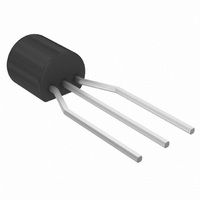
... BENT LEAD BULK PACK TAPE & REEL TO−92 (TO−226) AMMO PACK CASE 029 STYLE 10 MARKING DIAGRAMS MCR 22−x AYWW G G MCR22−x = Device Code Assembly Location Y = Year WW = Work Week G = Pb−Free Package (Note: Microdot may be in either location) PIN ASSIGNMENT 1 Cathode ...

Page 2

ELECTRICAL CHARACTERISTICS Characteristic OFF CHARACTERISTICS Peak Repetitive Forward or Reverse Blocking Current (V = Rated kW) AK DRM RRM GK ON CHARACTERISTICS Peak Forward On−State Voltage (Note Peak) ...

Page 3

CONDUCTION ANGLE 0.2 0.4 0.6 0.8 1.0 1 AVERAGE ON-STATE CURRENT (AMPS) T(AV) Figure 1. Maximum Case Temperature 5.0 3.0 2.0 1.0 0.7 0.5 0.3 0.2 0.1 0.07 ...

Page 4

T , JUNCTION TEMPERATURE ( C) J Figure 5. Typical Gate Trigger Voltage ...

Page 5

TO−92 EIA RADIAL TAPE IN FAN FOLD BOX OR ON REEL Item Tape Feedhole Diameter Component Lead Thickness Dimension Component Lead Pitch Bottom of Component to Seating Plane Feedhole Location Deflection Left or Right Deflection Front or ...

Page 6

... ORDERING & SHIPPING INFORMATION: MCR22 Series Packaging Options, Device Suffix Europe Equivalent U.S. MCR22−8RL1 MCR22−8RL1G MCR22−6 MCR22−6G MCR22−8 MCR22−8G MCR22−6RLRA MCR22−6RLRAG MCR22−6RLRP MCR22−6RLRPG †For information on tape and reel specifications, including part orientation and tape sizes, please refer to our Tape and Reel Packaging Specifications Brochure, BRD8011/D. † ...

Page 7

... B 4.32 5.33 C 3.18 4.19 D 0.40 0.54 G 2.40 2.80 J 0.39 0.50 K 12.70 --- N 2.04 2.66 P 1.50 4.00 R 2.93 --- V 3.43 --- STYLE 10: PIN 1. CATHODE 2. GATE 3. ANODE ON Semiconductor Website: www.onsemi.com Order Literature: http://www.onsemi.com/orderlit For additional information, please contact your local Sales Representative MCR22−6/D ...

Related keywords